
Infineon Technologies IRLZ34NL


- Part Number:
IRLZ34NL
- Manufacturer:
- Category:
- RoHs:
 Non-RoHS Compliant
 - Datasheet:
 IRLZ34NL_Datesheet
 - Description:
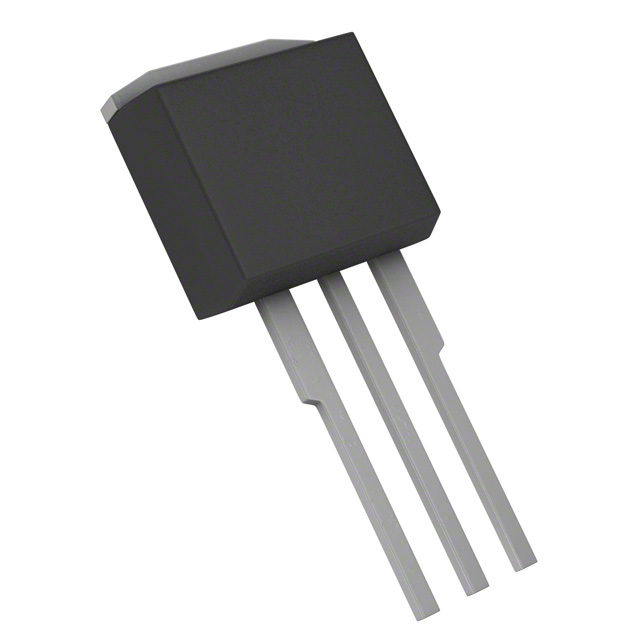
MOSFET N-CH 55V 30A TO262
- In stock 0

PRODUCT SPECIFICATION SUMMARY
Infineon HEXFET Power MOSFET - Part Number: IRLZ34NL
1. PART NUMBER DECODING
| Code Segment | Value | Description |
|---|---|---|
| IR | International Rectifier | Manufacturer identifier |
| L | Logic Level | Optimized for low gate drive voltage (4.5V) |
| Z | Z-Series | HEXFET technology family |
| 34 | Model number | Specific device identifier |
| N | N-Channel | Channel type |
| L | Lead-Free | RoHS compliant, lead-free TO-262 package |
2. PRODUCT OVERVIEW
Type: HEXFET N-Channel Power MOSFET
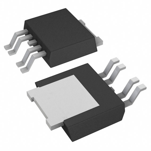
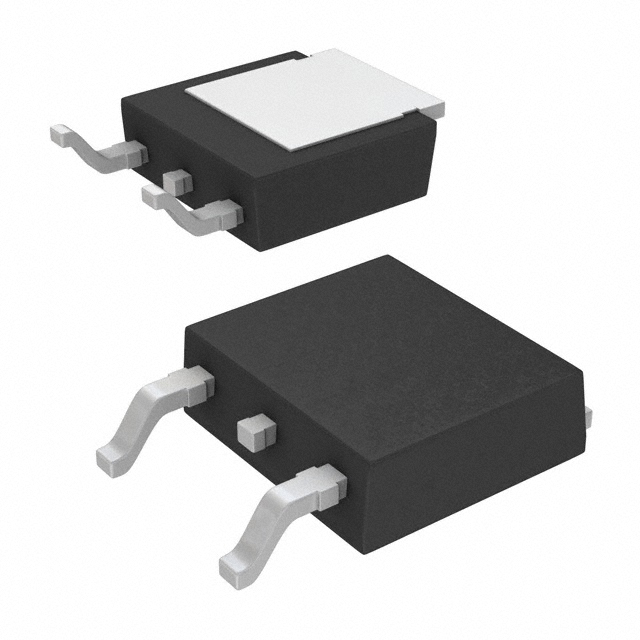
Package: TO-262 (D²PAK Through-Hole)
Technology: Logic-Level Gate Drive
Status: Active production
Key Features
- Logic-level gate drive (fully enhanced at 4.5V Vgs)
- Low on-resistance: 40 mΩ max at 10V gate drive
- High current capability: 27A continuous current
- Fast switching: Suitable for high-frequency applications
- Avalanche energy rated: Single-pulse avalanche energy rated for robust operation
- Lead-free and RoHS compliant
Typical Applications
- DC motor drives and servo control
- Power supplies: SMPS, DC-DC converters
- Automotive systems: Engine management, body electronics
- Lighting: LED drivers, HID ballasts
- Load switching: Solenoids, relays, power distribution
- Battery management systems
3. ABSOLUTE MAXIMUM RATINGS (TC = 25°C unless specified)
| Parameter | Symbol | Value | Unit |
|---|---|---|---|
| Drain-to-Source Voltage | V(BR)DSS | 55 | V |
| Continuous Drain Current (@ VGS=10V, TC=100°C) | ID | 27 | A |
| Continuous Drain Current (@ VGS=10V, TC=25°C) | ID | 19 | A |
| Pulsed Drain Current (t = 20µs) | IDM | 110 | A |
| Gate-to-Source Voltage | VGS | ±16 | V |
| Single Pulse Avalanche Energy (L=0.38mH, IAS=16A) | EAS | 48 | mJ |
| Repetitive Avalanche Energy | EAR | 8.3 | mJ |
| Power Dissipation (TC = 25°C) | PD | 68 | W |
| Linear Derating Factor | - | 0.45 | W/°C |
| Operating Junction Temperature | TJ | -55 to +175 | °C |
| Storage Temperature Range | TSTG | -55 to +175 | °C |
4. ELECTRICAL SPECIFICATIONS (TC = 25°C unless specified)
Static Characteristics
| Parameter | Symbol | Conditions | Min | Typ | Max | Unit |
|---|---|---|---|---|---|---|
| Drain-Source Breakdown Voltage | V(BR)DSS | VGS = 0V, ID = 250µA | 55 | - | - | V |
| Gate Threshold Voltage | VGS(th) | VDS = VGS, ID = 250µA | 1.0 | - | 2.0 | V |
| Static Drain-Source On-Resistance | RDS(on) | VGS = 10V, ID = 27A | - | - | 0.040 | Ω |
| Static Drain-Source On-Resistance | RDS(on) | VGS = 4.5V, ID = 13A | - | - | 0.045 | Ω |
| Static Drain-Source On-Resistance | RDS(on) | VGS = 4.0V, ID = 13A | - | - | 0.055 | Ω |
| Gate-Body Leakage Current | IGSS | VDS = 0V, VGS = ±16V | - | - | ±100 | nA |
| Zero Gate Voltage Drain Current | IDSS | VDS = 55V, VGS = 0V, TJ = 25°C | - | - | 1 | µA |
| Zero Gate Voltage Drain Current | IDSS | VDS = 55V, VGS = 0V, TJ = 125°C | - | - | 20 | µA |
| Forward Transconductance | gFS | VDS = 25V, ID = 16A | - | 25 | - | S |
5. THERMAL CHARACTERISTICS
| Parameter | Symbol | Value | Unit |
|---|---|---|---|
| Thermal Resistance, Junction-to-Case | RθJC | 2.2 | °C/W |
| Thermal Resistance, Junction-to-Ambient | RθJA | 50 | °C/W |
| Maximum Lead Temperature for Soldering | TL | 300 (for 10s) | °C |
6. DYNAMIC CHARACTERISTICS (TC = 25°C)
| Parameter | Symbol | Conditions | Min | Typ | Max | Unit |
|---|---|---|---|---|---|---|
| Input Capacitance | Ciss | VDS = 25V, VGS = 0V, f = 1.0MHz | - | 880 | - | pF |
| Output Capacitance | Coss | VDS = 25V, VGS = 0V, f = 1.0MHz | - | 120 | - | pF |
| Reverse Transfer Capacitance | Crss | VDS = 25V, VGS = 0V, f = 1.0MHz | - | 85 | - | pF |
7. SWITCHING CHARACTERISTICS (TC = 25°C, resistive load)
| Parameter | Symbol | Conditions | Min | Typ | Max | Unit |
|---|---|---|---|---|---|---|
| Turn-On Delay Time | td(on) | VDD = 28V, ID = 16A, RG = 4.7Ω, VGS = 10V | - | 10 | - | ns |
| Rise Time | tr | VDD = 28V, ID = 16A, RG = 4.7Ω, VGS = 10V | - | 36 | - | ns |
| Turn-Off Delay Time | td(off) | VDD = 28V, ID = 16A, RG = 4.7Ω, VGS = 10V | - | 25 | - | ns |
| Fall Time | tf | VDD = 28V, ID = 16A, RG = 4.7Ω, VGS = 10V | - | 24 | - | ns |
| Total Gate Charge | Qg | VDD = 44V, ID = 16A, VGS = 10V | - | 39 | 50 | nC |
| Threshold Gate Charge | Qgs | VDD = 44V, ID = 16A, VGS = 10V | - | 6.8 | - | nC |
| Plateau Gate Charge | Qgd | VDD = 44V, ID = 16A, VGS = 10V | - | 13 | - | nC |
8. BODY DIODE CHARACTERISTICS
| Parameter | Symbol | Conditions | Min | Typ | Max | Unit |
|---|---|---|---|---|---|---|
| Source-Drain Diode Voltage | VSD | IS = 16A, VGS = 0V, TJ = 25°C | - | - | 1.3 | V |
| Reverse Recovery Time | trr | IF = 16A, di/dt = 100A/µs | - | 85 | - | ns |
| Reverse Recovery Charge | Qrr | IF = 16A, di/dt = 100A/µs | - | 180 | - | nC |
| Forward Diode Current | ISD | - | - | - | 27 | A |
9. TYPICAL PERFORMANCE CHARACTERISTICS
On-Resistance vs. Temperature
- Rds(on) increases approximately 40% from 25°C to 125°C
- Normalized Rds(on) at 175°C: ~1.6× the value at 25°C
Safe Operating Area (SOA)
- Current limited by Rds(on): At low VDS
- Power dissipation limited: Moderate VDS region
- Avalanche energy limited: High voltage region
- Thermal limited: Continuous operation boundary
Capacitance Characteristics
- Ciss: Decreases with increasing VDS (from ~2500pF at 1V to ~200pF at 50V)
- Coss: Decreases significantly with VDS
- Crss: Strongly voltage-dependent, affects switching speed
Gate Charge
- Total gate charge: 39nC typical at VGS=10V
- Plateau voltage: ~5V (critical for driver design)
- Miller charge (Qgd): 13nC (affects switching losses)
10. PACKAGE INFORMATION
TO-262 (D²PAK Through-Hole) Dimensions
| Dimension | Min | Max | Unit |
|---|---|---|---|
| Overall Length | 10.70 | 10.90 | mm |
| Overall Width | 4.52 | 4.72 | mm |
| Overall Height | 4.10 (at flange) | - | mm |
| Lead Width | 0.55 | 0.75 | mm |
| Lead Thickness | 0.40 | 0.60 | mm |
| Lead Pitch | 2.21 | 2.59 | mm |
| Mounting Hole Diameter | 3.90 | 4.10 | mm |
Package Marking
- Line 1: International Rectifier Logo
- Line 2: Part Number (e.g., IRLZ34N)
- Line 3: Date Code (Year/Week)
- Line 4: Assembly Line Code
- Lead-Free Indicator: "P" in assembly line position
11. ORDERING INFORMATION
| Part Number | Package | Description | Lead-Free Status |
|---|---|---|---|
| IRLZ34NL | TO-262 | HEXFET N-Channel MOSFET | Lead-Free (RoHS) |
| IRLZ34NS | TO-263 (D²PAK SMD) | Same die, surface mount | Lead-Free (RoHS) Note: The "L" suffix indicates TO-262 through-hole package. "S" suffix indicates TO-263 surface mount package. |
12. SOLDERING & MOUNTING RECOMMENDATIONS
Through-Hole Mounting (TO-262)
- Mounting Screw: M3 or #4-40, torque 0.5-0.8 Nm
- Heat Sink: Recommended for PD > 5W
- Thermal Interface: Thermal grease or pad, 0.05mm max thickness
- Soldering: Wave soldering at 260°C max for 10 seconds
- Lead Forming: Bend at minimum 1.5mm from package body
Thermal Management
- RθJC: 2.2°C/W (junction-to-case)
- RθCS: 0.5-1.0°C/W typical (case-to-sink, with thermal interface)
- RθSA: Dependent on heatsink selecti
13. GATE DRIVE REQUIREMENTS
Minimum Drive Voltage
- Fully enhanced: VGS ≥ 4.5V for logic-level operation
- Standard drive: VGS = 10V for lowest Rds(on)
- Maximum: VGS ≤ 16V (absolute max)
Drive Power Calculation
- Gate drive power: Pdrive = Qg × VGS × fsw
- Example: At fsw=100kHz, VGS=10V → Pdrive = 39nC × 10V × 100kHz = 39mW
- Average gate current: Ig = Qg × fsw = 3.9mA at 100kHz
Driver Output Impedance
- Recommended: RG (external) + driver Rout should be ≤10Ω for fast switching
- Switching loss optimization: Balance between speed and EMI with gate resistor
14. RELIABILITY & QUALITY
Qualification Standards
- AEC-Q101: Qualified for automotive applications
- JEDEC: Compliant with J-STD-020, JESD51 standards
- Moisture Sensitivity: MSL Level 1 (unlimited floor life)
Avalanche Ruggedness
- Single-pulse avalanche energy: 48mJ (L=0.38mH, IAS=16A)
- Repetitive avalanche: 8.3mJ rated
- Unclamped inductive switching: Device can survive specified energy levels
Typical Failure Modes
- Electrical overstress: Exceeding VDS, VGS ratings
- Thermal runaway: Inadequate heatsinking
- Avalanche failure: Exceeding energy ratings
15. ENVIRONMENTAL COMPLIANCE
- RoHS Directive: Fully compliant (2011/65/EU)
- REACH: SVHC-free, compliant with EC 1907/2006
- Halogen-Free: Meets IEC 61249-2-21 standard
- Conflict Minerals: Compliant with Dodd-Frank Act Section 1502
- Green Packaging: Halogen-free mold compound
16. COMPARISON WITH RELATED PARTS
| Part Number | Package | VDS | ID | Rds(on) @ 10V | Logic Level | Notes |
|---|---|---|---|---|---|---|
| IRLZ34NL | TO-262 | 55V | 27A | 40mΩ | Yes | Through-hole |
| IRLZ34NS | TO-263 | 55V | 27A | 40mΩ | Yes | Surface mount |
| IRLZ44NL | TO-262 | 55V | 47A | 22mΩ | Yes | Higher current |
| IRF540N | TO-220 | 100V | 28A | 44mΩ | No | Standard gate drive |
17. DESIGN CONSIDERATIONS
Parallel Operation
- Gate resistors: Use individual gate resistors (4.7Ω-10Ω) for each device
- Current sharing: Match Rds(on) and thermal conditions
- Oscillation prevention: Minimize gate driver loop inductance
Protection Circuits
- Gate protection: Zener diode (16V) recommended for VGS clamping
- Overcurrent: Fast-acting fuse or current limiting
- Overvoltage: TVS diode for inductive load clamping
- ESD: Handle with proper ESD precautions (HBM Class 2)
Purchase
No need to register to order from JMChip Electronics, but signing in lets you track your order like a pro. Give it a try for a smoother shopping ride.
Means
Easy peasy! Pay your way with PayPal, Credit Card, or wire transfer in USD. We've got you covered.
RFQ(Request for Quotations)
Get the freshest prices and stock updates by asking for a quote! Our sales team will shoot you an email within a day. It's that simple.
IMPORTANT NOTICE
1. Look out for your order details in your inbox! (If it's missing, check the spam folder just in case.)
2. Our sales manager will double-check the order and keep you posted on any price or stock changes. No worries, we've got you covered.

Shipping Rate
We ship orders once a day around 5 p.m., except Sunday. Once shipped, the estimated delivery time depends on the courier company you choose, usually 5-7 working days.

Shipping Methods
We provide DHL, FedEx, UPS, EMS, SF Express, and Registered Air Mail international shipping.


Payment
You can pay the orders on the website directly or pay by wire transfer offline. We support: Paypal、VISA、Credit Card.


Infineon Technologies
Infineon Technologies
Infineon Technologies
Infineon Technologies
Infineon Technologies
Infineon Technologies
Infineon Technologies
Infineon Technologies
Infineon Technologies
Infineon Technologies
Infineon Technologies
Infineon Technologies