IXYS IXTU1N80P


- Part Number:
IXTU1N80P
- Manufacturer:
- Category:
- RoHs:
 Non-RoHS Compliant
 - Datasheet:
- Description:
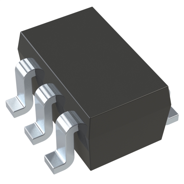
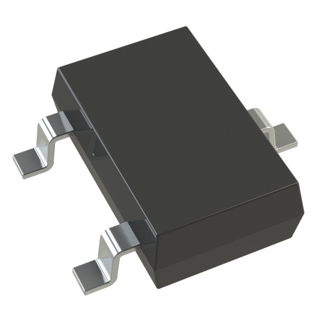
MOSFET N-CH TO251
- In stock 0

IXTU1N80P – 800V 1A N‑Channel Enhancement‑Mode Power MOSFET (Full Datasheet Summary)
1. Basic Information
- Manufacturer: IXYS (Littelfuse)
- Document: Preliminary Technical Information, DS100112A (June 2017)
- Device Type: N‑channel enhancement‑mode power MOSFET
- Package: TO‑251 (through‑hole plastic package)
- Key Specs: VDSS = 800 V, ID25 = 1 A, RDS(on) ≤ 14 Ω
- Marking: PolarTM series, avalanche rated
- Applications: DC‑DC converters, SMPS, motor drives, laser discharge, ignition circuits, high‑voltage pulse power
2. Key Features
- Avalanche‑energy rated (EAS = 75 mJ)
- Low gate charge (QG) for fast switching
- Low package inductance
- Fast intrinsic body diode
- Industry‑standard through‑hole package
- High power density
3. Absolute Maximum Ratings (TC = 25 °C, unless noted)
表格
| Parameter | Symbol | Value | Unit |
|---|---|---|---|
| Drain‑source voltage (TJ = 25–150 °C) | VDSS | 800 | V |
| Drain‑gate voltage (RGS = 1 MΩ) | VDGR | 800 | V |
| Gate‑source voltage (continuous) | VGSS | ±30 | V |
| Gate‑source voltage (transient) | VGSM | ±40 | V |
| DC drain current | ID25 | 1 | A |
| Peak drain current (pulse‑limited) | IDM | 2 | A |
| Avalanche current | IA | 1 | A |
| Avalanche energy | EAS | 75 | mJ |
| Drain‑source dv/dt | dv/dt | 5 | V/ns |
| Total power dissipation | PD | 42 | W |
| Junction / operating temperature | TJ, Tamb | −55 … +150 | °C |
| Storage temperature | Tstg | −55 … +150 | °C |
| Lead soldering temp (10 s, 1.6 mm from case) | TSOLD | 260 | °C |
| Max lead temp | TL | 300 | °C |
| Mounting force (TO‑251) | FC | 10–65 N | — |
| Weight | — | 0.40 | g |
4. Electrical Characteristics (TJ = 25 °C, unless noted)
Off Characteristics
表格
| Parameter | Symbol | Conditions | Min | Typ | Max | Unit |
|---|---|---|---|---|---|---|
| Drain‑source breakdown voltage | BVDSS | VGS = 0 V, ID = 250 μA | 800 | — | — | V |
| Gate threshold voltage | VGS(th) | VDS = VGS, ID = 50 μA | 2.0 | — | 4.0 | V |
| Gate‑source leakage | IGSS | VGS = ±30 V, VDS = 0 V | — | — | ±100 | nA |
| Drain‑source leakage | IDSS | VDS = VDSS, VGS = 0 V | — | — | 3 | μA |
| TJ = 125 °C | — | — | 30 | μA |
On Characteristics
表格
| Parameter | Symbol | Conditions | Min | Typ | Max | Unit |
|---|---|---|---|---|---|---|
| Drain‑source on‑resistance | RDS(on) | VGS = 10 V, ID = 0.5 A | — | 10 | 14 | Ω |
| Forward transconductance | gfs | VDS = 20 V, ID = 0.5 A | 0.30 | — | 0.55 | S |
Dynamic Characteristics
表格
| Parameter | Symbol | Conditions | Typ | Unit |
|---|---|---|---|---|
| Input capacitance | Ciss | VDS = 25 V, VGS = 0 V, f = 1 MHz | 250 | pF |
| Output capacitance | Coss | — | 58 | pF |
| Reverse transfer capacitance | Crss | — | 5.3 | pF |
| Total gate charge | Qg | VGS = 10 V, VDS = 400 V, ID = 0.5 A | 9.0 | nC |
| Gate‑source charge | Qgs | — | 1.4 | nC |
| Gate‑drain charge | Qgd | — | 5.5 | nC |
Switching Times (VGS = 10 V, RG = 50 Ω)
表格
| Parameter | Symbol | Typ | Unit |
|---|---|---|---|
| Turn‑on delay | td(on) | 22 | ns |
| Rise time | tr | 20 | ns |
| Turn‑off delay | td(off) | 18 | ns |
| Fall time | tf | 42 | ns |
Intrinsic Diode
表格
| Parameter | Symbol | Conditions | Value | Unit |
|---|---|---|---|---|
| Continuous source current | IS | VGS = 0 V | 1 | A |
| Peak source current | ISM | — | 4 | A |
| Diode forward voltage | VSD | IF = 1 A | 1.3 | V |
| Reverse recovery time | trr | IF = 1 A, −di/dt = 100 A/μs | 700 | ns |
5. Thermal Characteristics
表格
| Parameter | Symbol | Value | Unit |
|---|---|---|---|
| Thermal resistance, junction‑to‑case | RthJC | — | °C/W |
| Thermal resistance, case‑to‑sink | RthCS | — | °C/W |
6. Pin Configuration (TO‑251, Top View)
表格
| Pin | Label | Function | Notes |
|---|---|---|---|
| 1 | G | Gate | — |
| 2 | D | Drain | Tab = Drain |
| 3 | S | Source | — |
7. Package Outline (TO‑251)
- Format: Through‑hole plastic package
- Dimensions: Provided in inches + millimeters (standard TO‑251 form factor)
- Mounting: Standard through‑hole PCB assembly
8. Important Notes
- Preliminary data; specifications subject to change
- Avalanche rated for robust inductive switching
- Do not exceed absolute maximum ratings
- Follow proper ESD handling
- Not recommended for life‑support or safety‑critical systems without full qualification
Purchase
No need to register to order from JMChip Electronics, but signing in lets you track your order like a pro. Give it a try for a smoother shopping ride.
Means
Easy peasy! Pay your way with PayPal, Credit Card, or wire transfer in USD. We've got you covered.
RFQ(Request for Quotations)
Get the freshest prices and stock updates by asking for a quote! Our sales team will shoot you an email within a day. It's that simple.
IMPORTANT NOTICE
1. Look out for your order details in your inbox! (If it's missing, check the spam folder just in case.)
2. Our sales manager will double-check the order and keep you posted on any price or stock changes. No worries, we've got you covered.

Shipping Rate
We ship orders once a day around 5 p.m., except Sunday. Once shipped, the estimated delivery time depends on the courier company you choose, usually 5-7 working days.

Shipping Methods
We provide DHL, FedEx, UPS, EMS, SF Express, and Registered Air Mail international shipping.


Payment
You can pay the orders on the website directly or pay by wire transfer offline. We support: Paypal、VISA、Credit Card.