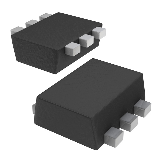
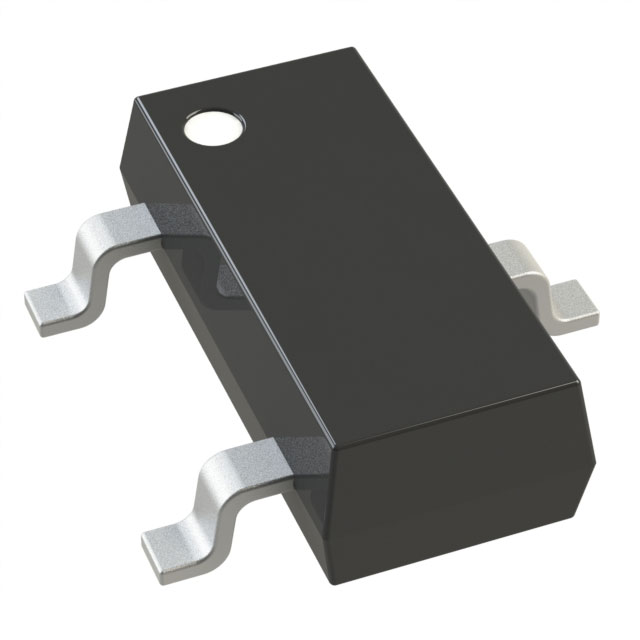
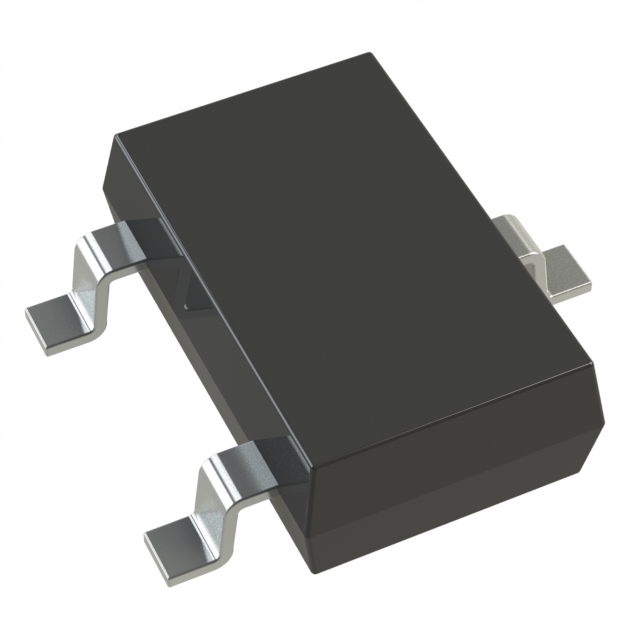
Motorola MTD3N25E


- Part Number:
MTD3N25E
- Manufacturer:
- Category:
- RoHs:
 Non-RoHS Compliant
 - Datasheet:
- Description:
N-CHANNEL POWER MOSFET
- In stock 4,500
MTD3N25E Datasheet Summary
General Description
The MTD3N25E is an N-Channel Enhancement-Mode Silicon Gate MOSFET designed for high energy withstand in avalanche and commutation modes. It features a fast recovery time drain-to-source diode, making it suitable for low voltage, high-speed switching applications in power supplies, converters, and PWM motor controls. The device is particularly well-suited for bridge circuits where diode speed and commutating safe operating areas are critical.
Features
- Avalanche Energy Specified
- Source-to-Drain Diode Recovery Time: Comparable to a Discrete Fast Recovery Diode
- Diode Characterized for Use in Bridge Circuits
- IDSS and VDS(on) Specified at Elevated Temperature
- Surface Mount Package Available: 16mm, 13-inch/2500 Unit Tape & Reel, Add T4 Suffix to Part Number
Ordering Information
- Part Number: MTD3N25E
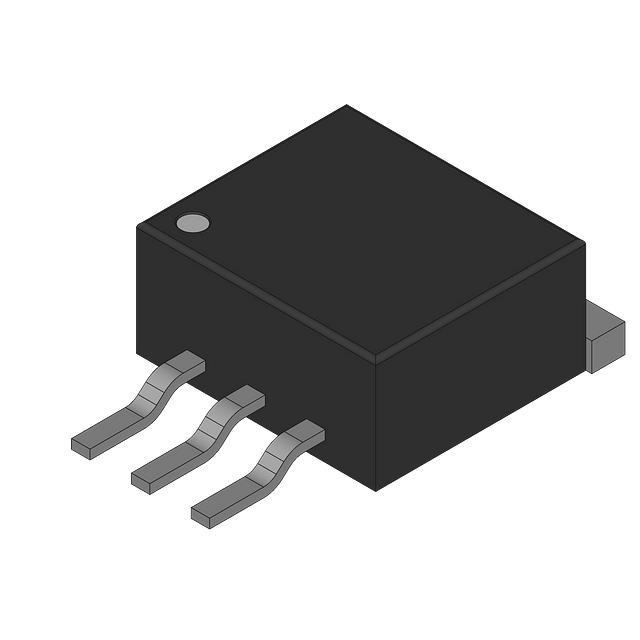
- Package: D2PAK (CASE 369A-13, Style 2DPAK)
- Operating Temperature Range: -55°C to +150°C
Electrical Characteristics (TJ = 25°C unless otherwise noted)
OFF CHARACTERISTICS
- Drain-Source Breakdown Voltage (V(BR)DSS): 250 Vdc
- Zero Gate Voltage Drain Current (IDSS): 10 µA (max) at 250 Vdc, 0 Vgs
- Gate-Body Leakage Current (IGSS): 100 nA (max) at ±20 Vdc, 0 Vds
ON CHARACTERISTICS
- Gate Threshold Voltage (VGS(th)): 2.0 to 6.0 Vdc
- Static Drain-Source On-Resistance (RDS(on)): 1.1 to 1.4 Ohms at 10 Vgs, 1.5 A
- Drain-Source On-Voltage (VDS(on)): 5.04 V (max) at 10 Vgs, 3.0 A
DYNAMIC CHARACTERISTICS
- Input Capacitance (Ciss): 307 to 430 pF at 1 MHz
- Output Capacitance (Coss): 57 to 75 pF at 25 Vdc, 0 Vgs, 1 MHz
- Reverse Transfer Capacitance (Crss): 14 to 25 pF at 25 Vdc, 0 Vgs, 1 MHz
SWITCHING CHARACTERISTICS
- Turn-On Delay Time (td(on)): 7.0 to 15 ns
- Rise Time (tr): 5.0 to 15 ns
- Turn-Off Delay Time (td(off)): 15 to 30 ns
- Fall Time (tf): 6.0 to 15 ns
- Gate Charge (QT): 9.8 to 15 nC
SOURCE–DRAIN DIODE CHARACTERISTICS
- Forward On-Voltage (VSD): 0.9 V (max) at 3.0 A, 0 Vgs
- Reverse Recovery Time (trr): 153 ns (max) at 3.0 A, 100 A/µs
- Reverse Recovery Stored Charge (QRR): 0.51 µC (max)
Maximum Ratings (TC = 25°C unless otherwise noted)
- Drain-Source Voltage (VDSS): 250 Vdc
- Drain-Gate Voltage (VDGR): 250 Vdc
- Gate-Source Voltage (VGS): ±20 Vdc
- Gate-Source Voltage (VGSM): ±40 Vdc (non-repetitive, tp ≤ 10 ms)
- Drain Current (ID): 3.0 A (continuous)
- Drain Current (IDM): 1.75 A (continuous @ 100°C)
- Drain Current (ID): 9.0 A (single pulse, tp ≤ 10 µs)
- Total Power Dissipation (PD): 40 W (TA = 25°C)
- Thermal Resistance (RθJC): 3.13 °C/W
- Thermal Resistance (RθJA): 100 °C/W
- Thermal Resistance (RθJA): 71.4 °C/W (mounted to minimum recommended pad size)
- Operating and Storage Temperature Range (TJ, Tstg): -55 to +150 °C
- Single Pulse Drain-to-Source Avalanche Energy (EAS): 45 mJ (starting TJ = 25°C)
Applications
- Power Supplies
- Converters
- PWM Motor Controls
- Bridge Circuits
Package Dimensions
- CASE 369A-13, Style 2DPAKDimensions: 13.2 mm x 6.5 mm x 1.27 mmLead Pitch: 1.27 mmLead Length: 1.27 mmLead Width: 0.51 mm
Purchase
No need to register to order from JMChip Electronics, but signing in lets you track your order like a pro. Give it a try for a smoother shopping ride.
Means
Easy peasy! Pay your way with PayPal, Credit Card, or wire transfer in USD. We've got you covered.
RFQ(Request for Quotations)
Get the freshest prices and stock updates by asking for a quote! Our sales team will shoot you an email within a day. It's that simple.
IMPORTANT NOTICE
1. Look out for your order details in your inbox! (If it's missing, check the spam folder just in case.)
2. Our sales manager will double-check the order and keep you posted on any price or stock changes. No worries, we've got you covered.

Shipping Rate
We ship orders once a day around 5 p.m., except Sunday. Once shipped, the estimated delivery time depends on the courier company you choose, usually 5-7 working days.

Shipping Methods
We provide DHL, FedEx, UPS, EMS, SF Express, and Registered Air Mail international shipping.


Payment
You can pay the orders on the website directly or pay by wire transfer offline. We support: Paypal、VISA、Credit Card.


