
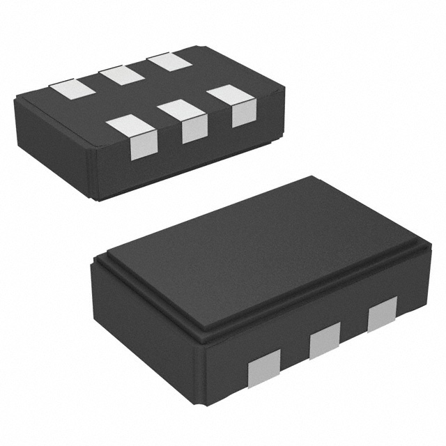
Categories
- Pin Configurable/Selectable Oscillators(1)


- 1
What is a pin configuration/selectable oscillator?
A pin configuration/selectable oscillator refers to the layout and positioning of the metal pins or terminals on an electronic component, enabling connections to other components or a printed circuit board. The pin configuration is essential because it dictates how the component can be connected to other parts and how it fits into a circuit design.
How to read a Pin Configuration Diagram?
A pin configuration diagram, often referred to as a pinout diagram, visually illustrates the pins or terminals of an electronic component along with their functions. Understanding how to interpret this diagram is crucial when working with electronic components. Here are the steps to follow:
Step 1: Identify the Component
Start by identifying the electronic component you need to reference. The component's name and part number will typically be found on the datasheet.
Step 2: Locate the Pin Configuration Diagram
Find the pin configuration diagram within the datasheet. It may be labeled as “Pinout,” “Pin Configuration,” or “Pin Connection Diagram.”
Step 3: Identify the Pin Numbering
The pin numbering assigns a unique identifier to each pin or terminal. Generally, the pins are numbered sequentially, beginning with pin one and progressing upwards. The numbers may be shown next to each pin or within the pin box in the diagram.
Step 4: Identify the Pin Functions
Each pin serves a specific purpose, and the pin configuration diagram will outline these functions, often indicated by labels next to the pins or inside the pin boxes. Some pins may have multiple functions, which will be noted with various labels.
Step 5: Identify the Pin Placement
Pin placement refers to the physical location of each pin on the component. The diagram may include an illustration or image of the component with each pin clearly labeled and numbered.
Step 6: Determine the Pin Connections
After identifying the pin functions, numbering, and placement, you can ascertain how to connect the component within the circuit. The diagram will indicate which pins need to be connected to other components or the circuit board.


