
Categories
- Single IGBTs(422)


- 1
- 2
- 3
- 4
- 5
- 6
- 22
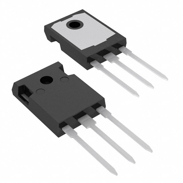
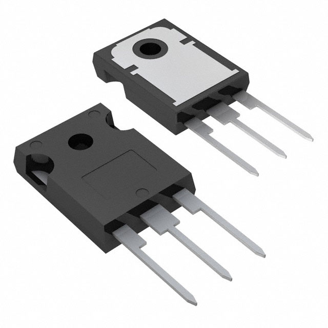
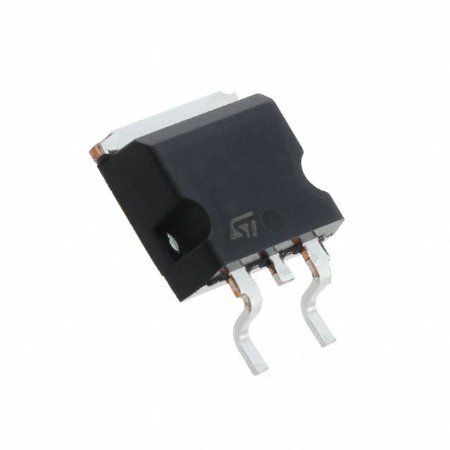
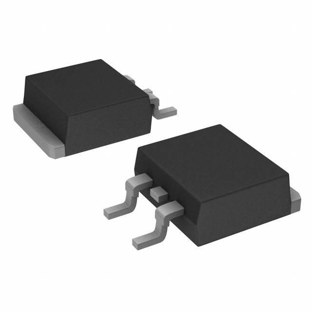
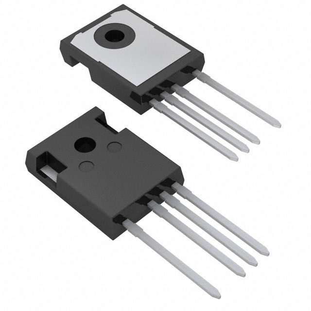
Single IGBTs (Insulated Gate Bipolar Transistors) are multilayer semiconductor devices featuring three terminals, capable of managing high currents and offering rapid switching capabilities. Their characteristics include type, collector-emitter breakdown voltage, collector current, pulsed collector current, VCE(ON), switching energy, and gate charge.
What is an IGBT?
The IGBT (Insulated Gate Bipolar Transistor) is a four-layer, three-terminal power semiconductor device that is a functional integration of a power MOSFET and a BJT for fast switching and higher power ratings. IGBTs offer lower on-state power loss and higher power ratings than MOSFETs and BJTs. The internal four-layer PNPN forms a MOSFET, a PNP, and an NPN transistor inside the structure. When the internal PNP transistor conducts the internal MOSFET, the IGBT begins to conduct.
How does an IGBT work?
IGBTs are similar in construction to power MOSFETs but operate like power BJTs because bipolar currents flow through electrons and holes. A power MOSFET only drives unipolar currents in the device. However, the physical structure of an IGBT is similar to that of an n-channel power MOSFET, but with the addition of an injection layer.
The gate terminal of the IGBT is connected to the emitter terminal through the battery. The emitter terminal is connected to the negative terminal of the battery and the gate terminal is connected to the positive terminal. The voltage drop between the emitter and gate terminals is referred to as V V GE. The voltage V GE is the input voltage to the control entity that controls the output collector current I C of the IGBT.
The collector terminal of the IGBT is connected to the emitter terminal through another battery. The collector terminal is connected to the positive terminal of the battery and the emitter terminal is connected to the negative terminal. The voltage drop between the emitter and collector terminals is called V CE. Voltage V CE is the output voltage of the IGBT device.


