
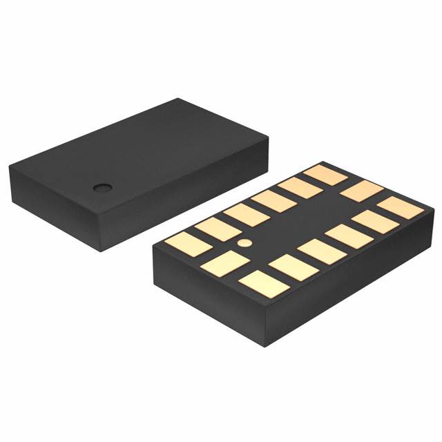
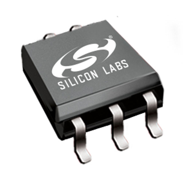
Murata Electronics SCR1100-D04-05


- Part Number:
SCR1100-D04-05
- Manufacturer:
- Category:
- RoHs:
 RoHS Compliant
 - Datasheet:
 SCR1100-D04-05_Datesheet
 - Description:
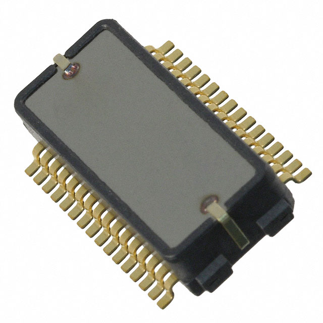
SENSOR GYRO 300DEG SNGL AXIS SPI
- In stock 0

SCR1100-D04-05 Product Information Summary
1. General Description
The SCR1100-D04-05 is a high-performance single-axis angular rate gyroscope developed by Murata, based on proven capacitive 3D-MEMS technology. It integrates a MEMS sensing element and a signal conditioning ASIC with a digital SPI interface, dedicated to measuring angular rate around the X-axis. With a measurement range of ±300 °/s, superior bias stability, and strong resistance to mechanical vibrations and shocks, it operates over an extended temperature range of -40 °C to +125 °C. Housed in a compact 8.5 x 18.7 x 4.5 mm (w x l x h) RoHS-compliant package, it supports SMD mounting and lead-free soldering. Factory-calibrated parameters (stored in non-volatile memory) ensure out-of-the-box usability, making it ideal for demanding applications such as inertial measurement units (IMUs), platform stabilization, robotic control, and navigation systems.
2. Core Features and Benefits
- Precise Angular Rate Measurement: ±300 °/s range with 18 LSB/(°/s) sensitivity and ±2% total sensitivity error, ensuring accurate motion detection.
- Superior Stability: Low bias instability (<2.1 °/h typical) and angular random walk (0.86 °/√h typical) for high-precision applications.
- Robust Environmental Performance: Resistant to vibrations and shocks (50g/6ms), with minimal cross-axis sensitivity (max 1.7%) and G-sensitivity (±0.1 (°/s)/g).
- Digital Interface: 4-wire SPI interface (0.1–8 MHz clock rate) supporting 16-bit data transfer and optional parity check (odd/even) for reliable communication.
- Dual Supply Operation: Analog supply (AVDD_G: 4.75–5.25 V) and digital supply (DVDD_G: 3.0–3.6 V) with low power consumption (analog: 26 mA typ; digital: 20 mA typ).
- Enhanced Diagnostics: Integrated self-diagnostics and status flags (S_OK) for real-time operation monitoring; parity error detection for SPI communication.
- Compact and Durable: Small form factor with robust packaging, thermal management via heat sink pins, and RoHS/ELV compliance.
- Fast Responsiveness: 50 Hz -3dB bandwidth, 2 kHz output data rate, and 0.8 s power-on setup time for real-time applications.
3. Applications
- Inertial Measurement Units (IMUs) for harsh environments
- Platform stabilization and control systems
- Motion analysis and robotic control
- Roll-over detection systems
- Guidance and navigation systems
- Industrial automation and precision motion control
4. Key Electrical Specifications
4.1 Performance Specifications (AVDD_G=5 V, DVDD_G=3.3 V, ambient temperature unless stated otherwise)
| Parameter | Condition | Min | Typ | Max | Unit |
|---|---|---|---|---|---|
| Measurement Range (X-axis) | - | -300 | - | 300 | °/s |
| Offset Error | - | -1.5 | - | 1.5 | °/s |
| Offset Over Temperature | -40 to +125 °C | -0.9 | - | 0.9 | °/s |
| Offset Over Temperature | -10 to +60 °C | -0.5 | - | 0.5 | °/s |
| Offset Drift Velocity | Temperature gradient ≤2.5 K/min | -0.6 | - | 0.6 | (°/s)/min |
| Short-Term Offset Instability | Constant temperature | - | <2.1 | - | °/h |
| Angular Random Walk (ARW) | - | - | 0.86 | - | °/√h |
| Sensitivity | - | - | 18 | - | LSB/(°/s) |
| Sensitivity Over Temperature | -40 to +125 °C | -1 | - | 1 | % |
| Total Sensitivity Error | - | -2 | - | 2 | % |
| Nonlinearity | -40 to +125 °C | -1 | - | 1 | °/s |
| RMS Noise | - | - | 0.14 | 0.23 | °/s |
| Noise Density | - | - | 0.02 | - | (°/s)/√Hz |
| Cross-Axis Sensitivity | - | - | - | 1.7 | % |
| G-Sensitivity | - | -0.1 | - | 0.1 | (°/s)/g |
| Shock Sensitivity | 50g, 6ms | - | - | 2.0 | °/s |
| Shock Recovery Time | - | - | - | 50.0 | ms |
| -3dB Bandwidth | - | - | 50 | - | Hz |
| Power-On Setup Time | - | - | - | 0.8 | s |
| Output Data Rate | - | - | 2 | - | kHz |
4.2 Absolute Maximum Ratings
| Parameter | Min | Max | Unit |
|---|---|---|---|
| Analog Supply Voltage (AVDD_G) | -0.5 | 7 | V |
| Digital Supply Voltage (DVDD_G) | -0.3 | 3.6 | V |
| Analog I/O Pin Voltage | -0.3 | AVDD_G + 0.3 | V |
| Digital I/O Pin Voltage | -0.3 | DVDD_G + 0.3 | V |
| Operating Temperature | -40 | 125 | °C |
| Storage Temperature | -40 | 125 | °C |
| Maximum Junction Temperature | - | 155 | °C |
| Mechanical Shock | - | 500 | g |
| ESD Protection (HBM) | - | 3000 | V |
| ESD Protection (CDM) | - | 2 | kV |
4.3 Power Consumption
| Parameter | Condition | Min | Typ | Max | Unit |
|---|---|---|---|---|---|
| Analog Supply Current (AVDD_G) | -40 to +125 °C | 24 | 26 | 29.5 | mA |
| Digital Supply Current (DVDD_G) | -40 to +125 °C | 16 | 20 | 24 | mA |
4.4 SPI Interface Specifications
4.4.1 DC Characteristics (DVDD_G=3.3 V)
| Parameter | Pin | Condition | Min | Typ | Max | Unit |
|---|---|---|---|---|---|---|
| Input High Voltage (VIH) | CSN_G, SCK_G, MOSI_G | - | 2.0 | - | DVDD_G | V |
| Input Low Voltage (VIL) | CSN_G, SCK_G, MOSI_G | - | 0 | - | 0.8 | V |
| Input Hysteresis (VHYST) | CSN_G, SCK_G, MOSI_G | - | 0.3 | - | - | V |
| Pull-Up Current (IPU) | CSN_G | VIN=0 V | 10 | - | 50 | µA |
| Pull-Down Current | MOSI_G | VIN=DVDD_G | 10 | - | 50 | µA |
| Input Leakage Current (ILEAK) | SCK_G | 0 < VIN < 3.3 V | -1 | - | 1 | µA |
| Output High Voltage (VOH) | MISO_G | IOUT=-1 mA | DVDD_G - 0.5 | - | - | V |
| Output High Voltage (VOH) | MISO_G | IOUT=-50 µA | DVDD_G - 0.2 | - | - | V |
| Output Low Voltage (VOL) | MISO_G | - | - | - | 0.5 | V |
| Capacitive Load | MISO_G | - | - | - | 200 | pF |
4.4.2 AC Characteristics (FSPI=8 MHz)
| Parameter | Min | Typ | Max | Unit |
|---|---|---|---|---|
| SCK_G High Time (TCH) | TSPI/2 | - | - | ns |
| SCK_G Low Time (TCL) | TSPI/2 | - | - | ns |
| CSN_G Setup Time (TLS1) | TSPI/2 | - | - | ns |
| CSN_G Hold Time (TLS2) | TSPI/2 | - | - | ns |
| MOSI_G Setup Time (TSET) | TSPI/4 | - | - | ns |
| MOSI_G Hold Time (THOL) | TSPI/4 | - | - | ns |
| CSN_G to MISO_G Delay (TVAL1) | TSPI/4 | - | - | ns |
| SCK_G to MISO_G Delay (TVAL2) | 1.3×TSPI/4 | - | - | ns |
| Tri-State Delay (TLZ) | TSPI/4 | - | - | ns |
| SCK_G Rise Time (TRISE) | - | - | 10 | ns |
| SCK_G Fall Time (TFALL) | - | - | 10 | ns |
| Inter-SPI Cycle Time (TLH) | TSPI | - | - | ns |
5. Pin Configuration and Description
5.1 Key Pin Definitions (32-Pin Package)
| Pin # | Name | Type | Description |
|---|---|---|---|
| 2 | REFGND_G | A1 | Analog reference ground; connect to AVSS_G externally. |
| 3 | VREFP_G | AO | Positive reference voltage output; max load 5 mA (for analog circuits only). |
| 4 | EXTRESN_G | DI (PU) | External reset (active low); Schmitt-trigger input with internal pull-up. |
| 6 | AHVVDDS_G | AO (HV) | High-voltage analog supply pad (~30 V); connect external capacitor. |
| 7 | LHV | AI (HV) | Inductor connection for high-voltage generation (~30 V). |
| 8 | DVDD_G | AI | Digital supply voltage (3.0–3.6 V). |
| 9 | DVSS_G | AI | Digital ground; connect to AVSS_G externally. |
| 10 | MISO_G | DOZ | SPI MISO (Master In Slave Out); 3.3 V level, tri-state output. |
| 23 | MOSI_G | DI (PD) | SPI MOSI (Master Out Slave In); 3.3 V Schmitt-trigger input with pull-down. |
| 24 | SCK_G | DI (PD) | SPI clock; 3.3 V Schmitt-trigger input (0.1–8 MHz) with pull-down. |
| 26 | CSN_G | DI (PU) | SPI chip select (active low); 3.3 V Schmitt-trigger input with pull-up. |
| 28 | AVDD_G | AI | Analog supply voltage (4.75–5.25 V). |
| 29 | SUB | AI | Substrate connection; connect to AVSS_G externally. |
| 1, 15, 18, 32 | HEAT | A1 | Heat sink pins; connect to AVSS_G for thermal management. |
| 5, 25, 27, 30, 31 | RESERVED | R | Factory use only; leave floating. |
| 11–14, 16, 17, 19–22 | NC | NC | Not connected; connect to GND or leave floating. |
6. Functional Operation
6.1 Core Working Principle
The MEMS sensing element uses vibrating masses excited into in-plane motion. Rotation around the X-axis induces out-of-plane movement, detected as capacitance changes by the ASIC. The ASIC conditions the signal, applies factory-calibrated parameters (sensitivity, offset over temperature), and outputs digital angular rate data via SPI.
6.2 Power-Up Sequence
- Apply DVDD_G (3.0–3.6 V) and wait 10 ms.
- Apply AVDD_G (4.75–5.25 V) and wait 800 ms (power-on setup time).
- Read the Status register (08h) twice to clear error flags.
- Angular rate data is immediately available; no additional initialization required.
6.3 Reset Mechanism
- Soft Reset: Write 0x04 to the IC Identification register (07h).
- Hard Reset: Trigger via EXTRESN_G pin (active low); ensure supplies are within range before releasing.
6.4 SPI Communication
- Transfer Protocol: 16-bit frames (address + data/status); MISO data shifts out on SCK falling edge, MOSI data sampled on SCK rising edge.
- Address Frame: D15–D9=0, D8–D2=register address (ADR6–ADR0), D1=RW (0=read, 1=write), D0=odd parity bit.
- Data Frame: 15-bit data (Dat14–Dat0) + 1-bit parity; write data stored in selected register, read data returned in subsequent frame.
- Parity Mode: Optional (enable via IC Identification register); 17-bit frames (16-bit data + parity bit) for error detection.
6.5 Key Registers
| Address (Hex) | Register Name | Function | Access |
|---|---|---|---|
| 00 | Rate_X | 14-bit angular rate data (two’s complement) + S_OK flag + parity bit | Read |
| 07 | IC Identification | Device ID, soft reset bit, parity enable (HWParEn), parity select (HWParSel) | Read/Write |
| 08 | Status/Config | Parity error flag (Parity_OK) + reserved factory-calibrated bits | Read |
| 0A | Temp | 14-bit temperature data (two’s complement) + S_OK flag + parity bit | Read |
6.6 Temperature Calculation
Temperature data (14-bit two’s complement) is factory-calibrated for offset; convert to °C using:\(Temp[°C] = (Temp[LSB] + 3250) / 65\)
- Typical output at +23 °C: -1755 counts
- Sensitivity: ~65 counts/°C
- Offset calibration error at 25 °C: ≤±15 °C
7. Package and Mechanical Specifications
7.1 Package Dimensions (mm)
| Parameter | Typ | Unit |
|---|---|---|
| Length (without leads) | 19.71 | mm |
| Width (without leads) | 8.5 | mm |
| Width (with leads) | 12.1 | mm |
| Height (with leads) | 4.60 | mm |
| Lead Pitch | 1.0 | mm |
7.2 PCB Footprint Dimensions (mm)
| Parameter | Typ | Unit |
|---|---|---|
| Footprint Length (without leads) | 15.7 | mm |
| Footprint Width (without leads) | 13.0 | mm |
| Lead Pitch (long side) | 1.0 | mm |
| Lead Length | 2.20 | mm |
| Lead Width (long side) | 0.7 | mm |
7.3 Thermal Characteristics
| Parameter | Max | Unit |
|---|---|---|
| Thermal Resistance (ΘJA) | 50 | °C/W |
8. Application Guidelines
8.1 Recommended External Components
| Component | Parameter | Min | Typ | Max | Unit |
|---|---|---|---|---|---|
| C1, C3, C5 | Capacitance | 70 | 100 | 130 | nF |
| C39 | Capacitance | 376 | 470 | 564 | nF |
| L1 | Inductance | 37 | 47 | 57 | µH |
| C6 | Capacitance | 0.7 | 1 | 1.3 | µF |
| Optional (PSRR Filter) | R1 | - | 10 | - | Ω |
| Optional (PSRR Filter) | C7 | - | 4.7 | - | µF |
| Optional (PSRR Filter) | L2 | - | 1k | - | Ω |
8.2 PCB Layout Recommendations
- Use separate analog/digital ground layers for long power supply lines; star connection for short lines.
- Place decoupling capacitors (C1, C3, C5, C6, C39) and inductor (L1) close to corresponding pins.
- Connect heat sink pins (HEAT) and SUB to AVSS_G for optimal thermal dissipation.
- Keep SPI lines short and matched to minimize noise; add optional RC/LC filter (R1, C7, L2) for unstable 3.3 V supplies.
8.3 Assembly Notes
- Compatible with lead-free soldering processes; validate PCB coating materials to avoid performance impact.
- Follow "Technical Note 82" for detailed assembly instructions.
- Avoid ultrasonic cleaning (prohibited per absolute maximum ratings).
Purchase
No need to register to order from JMChip Electronics, but signing in lets you track your order like a pro. Give it a try for a smoother shopping ride.
Means
Easy peasy! Pay your way with PayPal, Credit Card, or wire transfer in USD. We've got you covered.
RFQ(Request for Quotations)
Get the freshest prices and stock updates by asking for a quote! Our sales team will shoot you an email within a day. It's that simple.
IMPORTANT NOTICE
1. Look out for your order details in your inbox! (If it's missing, check the spam folder just in case.)
2. Our sales manager will double-check the order and keep you posted on any price or stock changes. No worries, we've got you covered.

Shipping Rate
We ship orders once a day around 5 p.m., except Sunday. Once shipped, the estimated delivery time depends on the courier company you choose, usually 5-7 working days.

Shipping Methods
We provide DHL, FedEx, UPS, EMS, SF Express, and Registered Air Mail international shipping.


Payment
You can pay the orders on the website directly or pay by wire transfer offline. We support: Paypal、VISA、Credit Card.


Murata Electronics
Murata Electronics
Murata Electronics
Murata Electronics
Murata Electronics
Murata Electronics
Murata Electronics
Murata Electronics
Murata Electronics
Murata Electronics
Murata Electronics
Murata Electronics