
Analog Devices Inc. AD9912ABCPZ


- Part Number:
AD9912ABCPZ
- Manufacturer:
- Category:
- RoHs:
 RoHS Compliant
 - Datasheet:
 AD9912ABCPZ_Datesheet
 - Description:
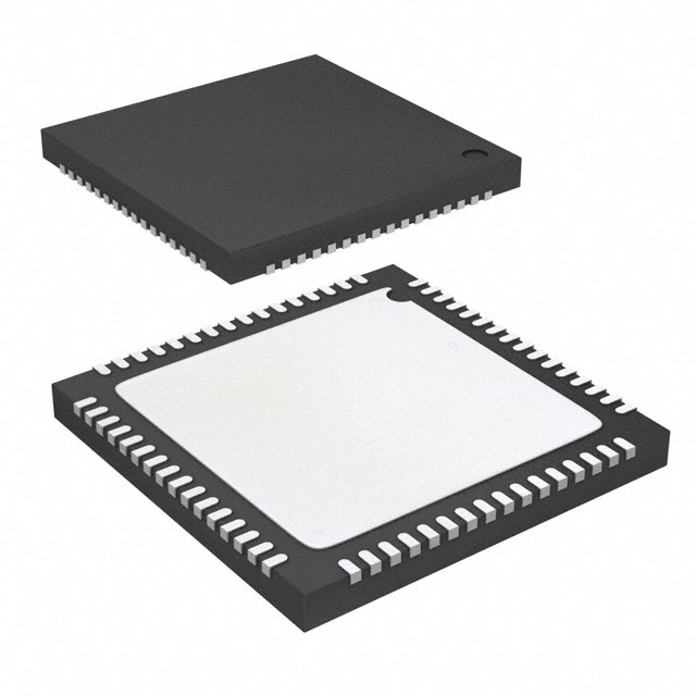
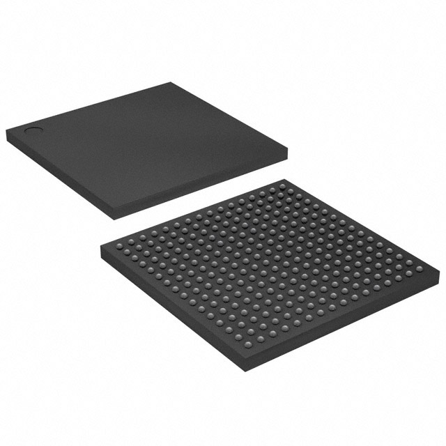
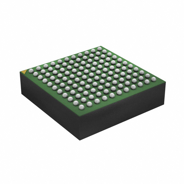
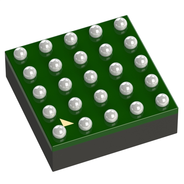
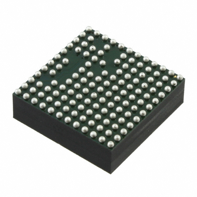
Direct Digital Synthesis IC 14 b 1 GHz 48 b Tuning 64-LFCSP-VQ (9x9)
- In stock 576

AD9912ABCPZ 1 GSPS Direct Digital Synthesizer (DDS) with 14-Bit DAC Specifications
Basic Information
- Part Number: AD9912ABCPZ
- Product Category: Direct Digital Synthesizer (DDS) with Integrated DAC
- Core Function: High-performance frequency synthesis with digital-to-analog conversion
- RoHS Compliance: Yes (denoted by "Z" in part number)
- Operating Temperature Range: -40°C to +85°C (industrial grade)
- Package Type: 64-lead Lead Frame Chip Scale Package (LFCSP), 9 mm × 9 mm body, 0.75 mm height (Package Option: CP-64-22)
- Key Features:
Electrical Specifications
Supply Voltage & Current
| Supply Rail | Voltage Range | Typical Current | Test Conditions |
|---|---|---|---|
| AVDD (Analog) | 1.71 V ~ 1.89 V (±5% of 1.8 V) | 40 mA (aggregate) | Digital core, SpurKiller off |
| AVDD3 (DAC/CMOS Driver) | 3.135 V ~ 3.465 V (±5% of 3.3 V); Pin 37 configurable to 1.8 V | 26 mA (Pin 46/47/49) | DAC output current source, fₛ=1 GSPS |
| DVDD (Digital Core) | 1.71 V ~ 1.89 V (±5% of 1.8 V) | 205 mA | Digital core, 1 GHz system clock |
| DVDD_I/O (Digital I/O) | 3.135 V ~ 3.465 V (±5% of 3.3 V) | 113 mA | Digital I/O, dynamic operation |
System Clock Input
- Modes: PLL Bypassed, PLL Enabled (external signal), Crystal Resonator (PLL Enabled)
- PLL Bypassed Input Range: 250 MHz ~ 1 GHz (differential/single-ended, ac-coupled)
- PLL Enabled Input Range: 25 MHz ~ 200 MHz (with doubler); VCO ranges: Low (700-810 MHz), Auto (810-900 MHz), High (900-1000 MHz)
- Crystal Compatibility: 25 MHz, 3.2 mm × 2.5 mm AT cut (max motional resistance 100 Ω)
DAC Output Characteristics
- Frequency Range (1st Nyquist Zone): 0 MHz ~ 450 MHz
- Output Resistance: 50 Ω (single-ended, internally terminated to AVSS)
- Output Capacitance: 5 pF
- Full-Scale Output Current: 8.6 mA ~ 31.7 mA (10-bit granularity), default 20 mA
- Gain Error: ±10% FS
- Wideband SFDR: -59 dBc ~ -79 dBc (0 MHz ~ 500 MHz)
- Narrow-Band SFDR: -86 dBc ~ -96 dBc (±250 kHz offset)
Clock Output Drivers
HSTL Driver (1.8 V Differential)
- Frequency Range: 20 MHz ~ 725 MHz (up to 622.08 MHz OC-12 rate)
- Differential Output Swing: 1080 mV ~ 1480 mV (static)
- Rise/Fall Time (20%-80%): 115 ps ~ 165 ps (100 Ω load, 2 pF)
- Jitter (12 kHz-20 MHz): 1.5 ps ~ 1.6 ps
- Subharmonic Spur Level: -35 dBc (without correction)
CMOS Driver (1.8 V/3.3 V Single-Ended)
- Frequency Range: <150 MHz
- Output Swing (3.3 V): VOH ≥2.7 V, VOL ≤0.4 V (I OH/I OL=1 mA)
- Output Swing (1.8 V): VOH ≥1.4 V, VOL ≤0.4 V (I OH/I OL=1 mA)
- Rise/Fall Time (20%-80%): 3 ns ~ 4.6 ns (20 pF load)
- Duty Cycle: 45% ~ 65%
Phase Noise (250 MHz Output, HSTL Driver)
- 10 Hz offset: -113 dBc/Hz
- 1 kHz offset: -133 dBc/Hz
- 100 kHz offset: -153 dBc/Hz
- 40 MHz offset: -161 dBc/Hz
Power Dissipation
| Operating Mode | Typical (mW) | Maximum (mW) | Test Conditions |
|---|---|---|---|
| DDS Only | 637 | 765 | SYSCLK=1 GHz, PLL bypassed, drivers off |
| DDS + Spur Reduction | 686 | 823 | Both SpurKiller channels enabled |
| DDS + HSTL Driver | 657 | 788 | HSTL driver active |
| DDS + CMOS Driver | 729 | 875 | CMOS driver + S-divider (f OUT=50 MHz) |
| Power-Down Mode | 13 | 16 | Via register or PWRDOWN pin |
Mechanical & Thermal Specifications
Package Dimensions (mm)
- Body Size: 9.00 (±0.10) × 9.00 (±0.10)
- Package Height: 0.75
- Exposed Pad Size: 5.21 (±0.15) × 5.21 (±0.15)
- Lead Diameter: 0.18 ~ 0.30
- Coplanarity: 0.08 max
Thermal Resistance (Typical, 64-lead LFCSP)
- θJA (Junction-to-Ambient): 25.2 °C/W (still air)
- θJB (Junction-to-Board): 13.9 °C/W (moving air)
- θJC (Junction-to-Case): 1.7 °C/W
- Note: Exposed pad must be soldered to ground for specified thermal performance.
Key Functional Blocks
Direct Digital Synthesizer (DDS)
- FTW Resolution: 48-bit, f_DDS = (FTW / 2⁴⁸) × fₛ
- Phase Control: 14-bit programmable phase offset (ΔΦ = 2π × Δphase / 2¹⁴)
- Power-Up Default Frequencies: 16 preprogrammed options (38.88 MHz ~ 155.52 MHz) via S1-S4 pins
Spur Reduction (SpurKiller)
- 2 independent channels (Spur A/B) for 2nd ~ 15th harmonic reduction
- 8-bit amplitude control + gain ×2 option; 9-bit phase control (±π)
- Typical performance improvement: 6 dB ~ 8 dB (common settings); up to 30 dB (manual tuning)
Serial Control Port
- Interface: 3-wire (default, SDIO) or 4-wire (SDO active)
- Instruction Word: 16-bit (R/W, transfer length, 13-bit address)
- Transfer Modes: MSB-first (default) or LSB-first; streaming mode supported
- Key Pins: SCLK (Pin 64), SDIO (Pin 63), SDO (Pin 62), CSB (Pin 61, active low)
CMOS Output Divider (S-Divider)
- Divide Ratio: 1 ~ 65,535 (base) or 2 ~ 131,070 (with /2 prescaler)
- Trigger Edge: Programmable rising/falling edge
- Required Setting: S-divider/2 bit (Register 0x0106, Bit 0) for FDBK_IN > 400 MHz
Pin Configuration (Key Pins)
| Pin Number | Pin Type | Mnemonic | Description |
|---|---|---|---|
| 27/28 | I (Diff) | SYSCLK/SYSCLKB | System clock input (differential pair) |
| 31 | O | LOOP_FILTER | PLL loop filter (pull down to GND when PLL bypassed) |
| 34/35 | O (Diff) | OUTB/OUT | HSTL differential output |
| 38 | O | OUT_CMOS | CMOS output (1.8 V/3.3 V configurable) |
| 40/41 | I (Diff) | FDBK_INB/FDBK_IN | Feedback inputs (ac-coupled, internally biased to ~1 V) |
| 48 | O | DAC_RSET | DAC current-set resistor (10 kΩ recommended to GND) |
| 50/51 | O (Diff) | DAC_OUT/DAC_OUTB | DAC differential output (50 Ω internal pull-down) |
| 58 | I | PWRDOWN | Power-down (active high, internal 50 kΩ pull-down) |
| 59 | I | RESET | Chip reset (active high, internal 10 kΩ pull-down) |
| 60 | I | IO_UPDATE | I/O register update trigger |
| Exposed Pad | O | EPAD | Analog ground (must be soldered to GND) |
Applications
- Agile LO frequency synthesis
- Low-jitter, fine-tune clock generation
- Test and measurement equipment
- Wireless base stations and controllers
- Secure communications
- Fast frequency hopping
Purchase
No need to register to order from JMChip Electronics, but signing in lets you track your order like a pro. Give it a try for a smoother shopping ride.
Means
Easy peasy! Pay your way with PayPal, Credit Card, or wire transfer in USD. We've got you covered.
RFQ(Request for Quotations)
Get the freshest prices and stock updates by asking for a quote! Our sales team will shoot you an email within a day. It's that simple.
IMPORTANT NOTICE
1. Look out for your order details in your inbox! (If it's missing, check the spam folder just in case.)
2. Our sales manager will double-check the order and keep you posted on any price or stock changes. No worries, we've got you covered.

Shipping Rate
We ship orders once a day around 5 p.m., except Sunday. Once shipped, the estimated delivery time depends on the courier company you choose, usually 5-7 working days.

Shipping Methods
We provide DHL, FedEx, UPS, EMS, SF Express, and Registered Air Mail international shipping.


Payment
You can pay the orders on the website directly or pay by wire transfer offline. We support: Paypal、VISA、Credit Card.


Analog Devices Inc.
Analog Devices Inc.
Analog Devices Inc.
Analog Devices Inc.
Analog Devices Inc.
Analog Devices Inc.
Analog Devices Inc.
Analog Devices Inc.
Analog Devices Inc.
Analog Devices Inc.
Analog Devices Inc.
Analog Devices Inc.