
Nexperia USA Inc. 74LVC1G14GW-Q100,1


- Part Number:
74LVC1G14GW-Q100,1
- Manufacturer:
- Category:
- RoHs:
 RoHS Compliant
 - Datasheet:
 74LVC1G14GW-Q100,1_Datesheet
 - Description:
IC INVERT SCHMITT 1CH 1IN 5TSSOP
- In stock 18,066

74LVC1G14GW-Q100 Datasheet Summary
General Information
- Manufacturer: Nexperia
- Part Number: 74LVC1G14GW-Q100
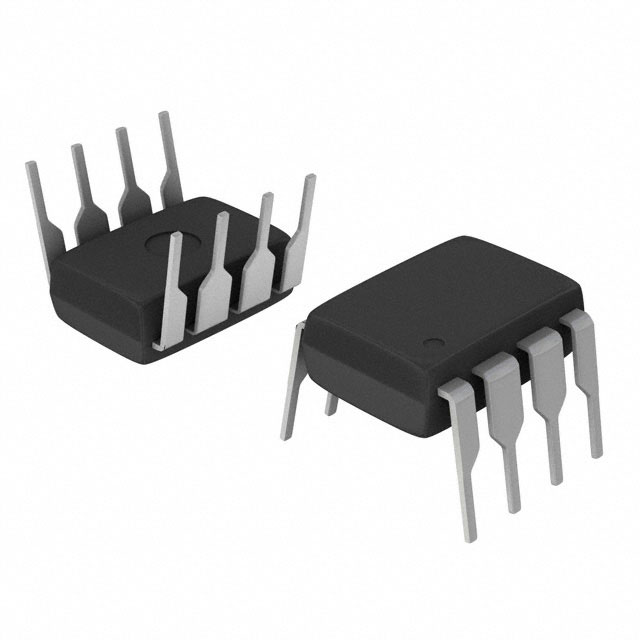
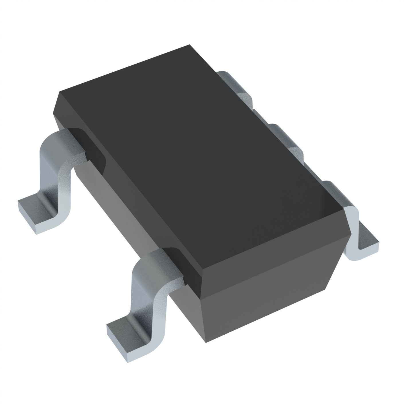
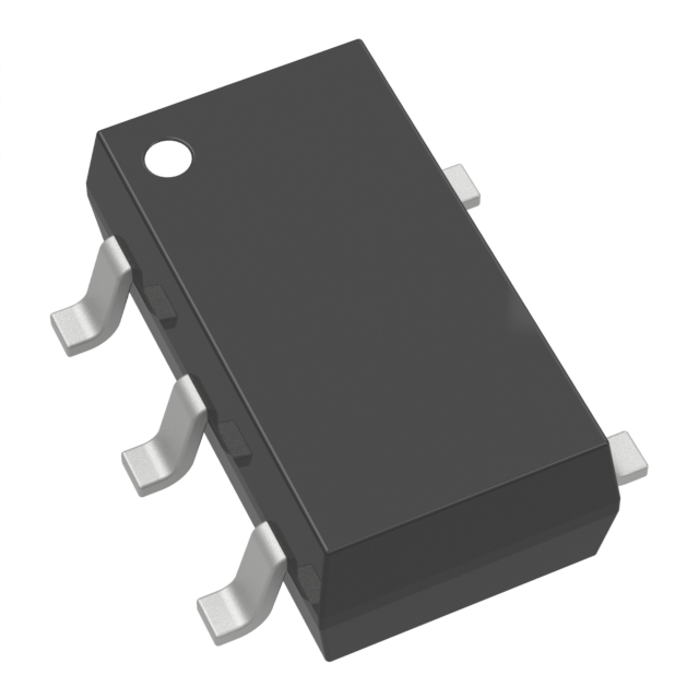
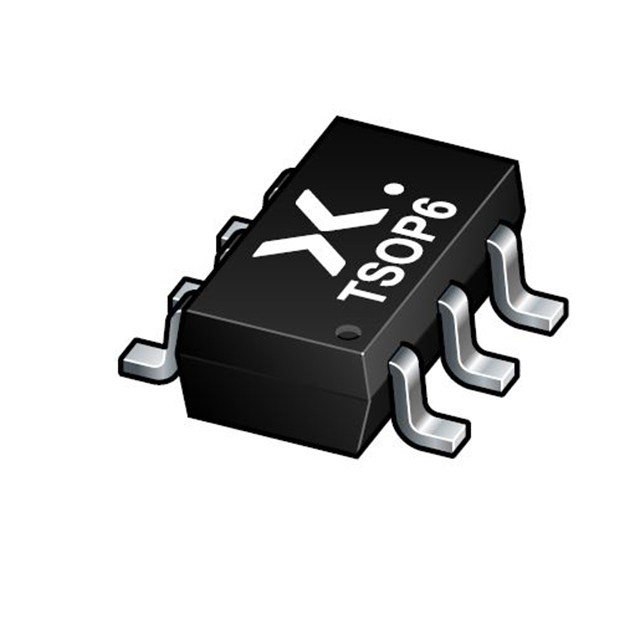
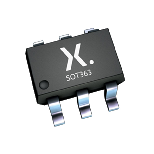
- Package Type: TSSOP5 (SOT353-1)
- Temperature Range: -40°C to +125°C
- Shipping Quantity: 5000 per Tape & Reel
Description
The 74LVC1G14GW-Q100 is a single Schmitt trigger inverter designed for automotive applications. It features a wide supply voltage range and is qualified to the Automotive Electronics Council (AEC) standard Q100 (Grade 1). The device supports input voltages from 3.3V or 5V devices, making it suitable for mixed voltage environments. It also includes IOFF circuitry to prevent backflow current during power-down.
Features
- Automotive Qualification: AEC-Q100 (Grade 1)
- Wide Supply Voltage Range: 1.65V to 5.5V
- Overvoltage Tolerant Inputs: Up to 5.5V
- High Noise Immunity
- CMOS Low Power Dissipation
- IOFF Circuitry: Partial Power-down mode operation
- Output Drive: ±24mA (VCC = 3.0V)
- Latch-up Performance: Exceeds 250mA
- Direct Interface with TTL Levels
- Unlimited Rise and Fall Times
- Compliance with JEDEC Standards:JESD8-7 (1.65V to 1.95V)JESD8-5 (2.3V to 2.7V)JESD8C (2.7V to 3.6V)JESD36 (4.5V to 5.5V)
- ESD Protection:HBM: Exceeds 2000VCDM: Exceeds 1000V
- Multiple Package Options
Applications
- Wave and pulse shaper
- Astable multivibrator
- Monostable multivibrator
Ordering Information
- Part Number: 74LVC1G14GW-Q100
- Package: TSSOP5 (SOT353-1)
- Temperature Range: -40°C to +125°C
- Shipping Quantity: 5000 per Tape & Reel
Marking
- Marking Code: VF
Pinning Information
TSSOP5 (SOT353-1) Pin Configuration
TableCopy
| Pin No. | Symbol | Description |
|---|---|---|
| 1 | n.c. | Not connected |
| 2 | VCC | Supply voltage |
| 3 | A | Data input |
| 4 | GND | Ground (0V) |
| 5 | Y | Data output |
Functional Description
- Input to Output Logic:A = LOW (L) -> Y = HIGH (H)A = HIGH (H) -> Y = LOW (L)
Limiting Values
- Supply Voltage (VCC): -0.5V to +6.5V
- Input Voltage (VI): -0.5V to +6.5V
- Output Voltage (VO): -0.5V to +6.5V
- Input Clamping Current (IIK): ±50mA
- Output Clamping Current (IOK): ±50mA
- Output Current (IO): ±50mA
- Supply Current (ICC): +100mA
- Ground Current (IGND): -100mA
- Storage Temperature (Tstg): -65°C to +150°C
- Total Power Dissipation (Ptot): 250mW (derates linearly with temperature)
Recommended Operating Conditions
- Supply Voltage (VCC): 1.65V to 5.5V
- Input Voltage (VI): 0V to 5.5V
- Output Voltage (VO): 0V to 5.5V
- Ambient Temperature (Tamb): -40°C to +125°C
Static Characteristics
- High-Level Output Voltage (VOH): VCC - 0.1V to VCC - 0.1V
- Low-Level Output Voltage (VOL): 0.10V to 0.10V
- Input Leakage Current (II): ±0.1μA to ±1μA
- Power-Off Leakage Current (IOFF): ±0.1μA to ±2μA
- Supply Current (ICC): 0.1μA to 4μA
- Additional Supply Current (ΔICC): 5μA to 500μA
- Input Capacitance (CI): 5.0pF
Dynamic Characteristics
- Propagation Delay (tpd): 0.7ns to 14.0ns (depending on VCC)
- Power Dissipation Capacitance (CPD): 15.4pF
Package Outline
TSSOP5 (SOT353-1) Dimensions
- Length (A): 1.1mm to 1.3mm
- Width (D): 2.2mm to 2.4mm
- Height (E): 1.7mm to 1.8mm
- Lead Length (Lp): 0.8mm to 1.0mm
- Lead Width (w): 0.6mm to 0.8mm
- Lead Thickness (v): 0.3mm to 0.5mm
Abbreviations
- ANSI: American National Standards Institute
- CDM: Charged Device Model
- CMOS: Complementary Metal Oxide Semiconductor
- DUT: Device Under Test
- ESD: ElectroStatic Discharge
- ESDA: ElectroStatic Discharge Association
- HBM: Human Body Model
- JEDEC: Joint Electron Device Engineering Council
- TTL: Transistor-Transistor Logic
Purchase
No need to register to order from JMChip Electronics, but signing in lets you track your order like a pro. Give it a try for a smoother shopping ride.
Means
Easy peasy! Pay your way with PayPal, Credit Card, or wire transfer in USD. We've got you covered.
RFQ(Request for Quotations)
Get the freshest prices and stock updates by asking for a quote! Our sales team will shoot you an email within a day. It's that simple.
IMPORTANT NOTICE
1. Look out for your order details in your inbox! (If it's missing, check the spam folder just in case.)
2. Our sales manager will double-check the order and keep you posted on any price or stock changes. No worries, we've got you covered.

Shipping Rate
We ship orders once a day around 5 p.m., except Sunday. Once shipped, the estimated delivery time depends on the courier company you choose, usually 5-7 working days.

Shipping Methods
We provide DHL, FedEx, UPS, EMS, SF Express, and Registered Air Mail international shipping.


Payment
You can pay the orders on the website directly or pay by wire transfer offline. We support: Paypal、VISA、Credit Card.


Nexperia USA Inc.
Nexperia USA Inc.
Nexperia USA Inc.
Nexperia USA Inc.
Nexperia USA Inc.
Nexperia USA Inc.
Nexperia USA Inc.
Nexperia USA Inc.
Nexperia USA Inc.
Nexperia USA Inc.
Nexperia USA Inc.
Nexperia USA Inc.