
ams OSRAM AS1332-BWLT


- Part Number:
AS1332-BWLT
- Manufacturer:
- Category:
- RoHs:
 Non-RoHS Compliant
 - Datasheet:
 AS1332-BWLT_Datesheet
 - Description:
IC REG CONV RF PWR 1OUT 8WLCSP
- In stock 0

AS1332-BWLT – austriamicrosystems
650 mA, 2 MHz Step-Down DC-DC Converter for RF Power Amplifiers
Complete Quick-Reference Datasheet Summary
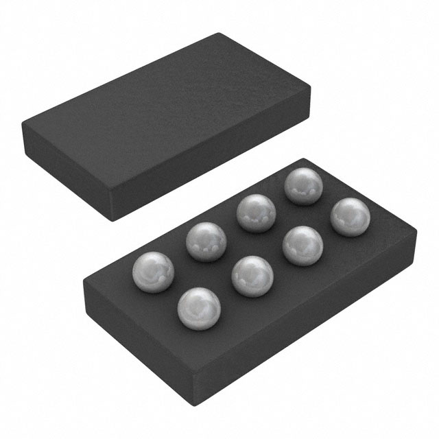
- Device IdentificationOrdering Code: AS1332-BWLTPackage: 8-pin WL-CSP (Wafer-Level Chip-Scale)Package Marking: ASQWRoHS / Pb-free: YesTape & Reel: 7-in reel, 3 k pcs typical
- Description & Target Applications
- Synchronous buck converter optimized to power RF PAs in Li-Ion–powered handsets
- Dynamic 1.3 V – 3.16 V output set by analog VCON pin (gain = 2.5 V/V)
- 2 MHz fixed-PWM operation → tiny passives, low output ripple, EMI-friendly
- 96 % peak efficiency (3.6 VIN, 3.16 VOUT, 400 mA)
- < 0.01 µA shutdown current
- Ideal for: cellular phones, handheld radios, RF PC-cards, battery-powered RF modules
- Absolute Maximum Ratings (stress only)PVIN, VDD to AGND ........................ –0.3 V → +7 VEN, FB, VCON .............................. –0.3 V → VDD+0.3 V (≤ 7 V)SW ........................................ –0.3 V → PVIN+0.3 VTJ max .................................... +150 °CTstg ....................................... –65 °C → +150 °CESD HBM ................................... 2 kV
- Operating Range (functional)VIN ........................................ 2.7 V – 5.5 V (single Li-Ion cell)Iload max ................................. 650 mA (PWM mode)TA ......................................... –40 °C → +85 °CTJ (recommended) .......................... –40 °C → +125 °C
- Electrical Characteristics (TJ = 25 °C, VIN = 3.6 V unless noted)
- Feedback / Output
VFB,min (VCON = 0.4 V) ................... 1.21 V min, 1.30 V typ, 1.39 V max
VFB,max (VCON = 1.27 V) ................. 3.03 V min, 3.17 V typ, 3.29 V max
Gain (VOUT vs VCON) ...................... 2.5 V/V (linear range 0.556 V ≤ VCON ≤ 1.208 V) - Supply Currents
IQ (no switching) .......................... 1 mA typ, 1.4 mA max
ISHDN (EN = 0 V) .......................... 0.01 µA typ, 2 µA max - Power Switches
PFET RDS(on) .............................. 140 mΩ typ / 200 mΩ max @ 200 mA, 25 °C
NFET RDS(on) .............................. 300 mΩ typ / 415 mΩ max @ –200 mA, 25 °C
Peak current limit ........................ 1.1 A typ, 0.935 A min, 1.2 A max
FOSC ...................................... 2 MHz typ (1.8 – 2.2 MHz over temp) - Control Inputs
EN VIH .................................... 1.2 V min
EN VIL .................................... 0.5 V max
VCON input resistance ..................... 100 kΩ typ
VCON leakage .............................. ±10 µA - Typical System Performance (@ 25 °C)
- Turn-on time (EN ↑ → 3.16 V) ........... 210 µs typ, 750 µs max
- VCON response (1.3 V → 3.16 V) ......... 30 µs typ
- Load transient (10 mA ↔ 400 mA) ........ ±50 mV deviation, <20 µs recovery
- Output ripple (PWM, 200 mA) ............ 10 mVPP typ
- PSRR (10 kHz, 100 mVPP) ................ 40 dB typ
- Functional Description
- Current-mode buck with synchronous rectification → no external Schottky
- VCON analog input directly sets VOUT (clamped below 0.484 V and above 1.312 V)
- Cycle-by-cycle 1.2 A valley current limit; timed hiccup when VOUT < 0.375 V
- Soft-start & thermal shutdown @ +150 °C (hysteresis ≈ 15 °C)
- Fixed 2 MHz allows 3.3 µH inductor, 0805/0603 ceramic caps
- Recommended External ComponentsL1 .......................................... 3.3 µH (±20 %), DCR ≤ 100 mΩ, sat ≥ 1.5 AExample: Coilcraft LPS4018-332ML_ (3.9 mm × 3.9 mm × 1.7 mm)CIN ........................................ 10 µF ±20 %, X5R/X7R, 6.3 V or 16 VExample: Murata GRM21BR60J106KE19 (0805)COUT ....................................... 4.7 µF ±20 %, X5R/X7R, 6.3 V – 16 VExample: Murata GRM21BR61C475KA88 (0805)Optional larger COUT (≤ 22 µF) lowers ripple & improves transients.
- Pinout (8-bump WL-CSP, 0.4 mm pitch)
- A1 PVIN – Power input to PFET switch
A2 SW – Switch node (inductor connection)
A3 PGND – Power ground
B1 VDD – Analog supply (bypass to AGND)
B3 AGND – Analog ground (Kelvin to PGND)
C1 EN – Enable (active-high, 1.2 V threshold)
C2 VCON – Analog control voltage (0.52 V – 1.27 V)
C3 FB – Feedback / output sense (connect to COUT +) - Typical Application CircuitLi-Ion 2.7-5.5 V+–– PVIN (A1)| +–– VDD (B1)| | +10 µF| | || +–– EN (C1) ← MCU GPIO| || +–– VCON (C2) ← DAC / PWM filtered| |+–– L 3.3 µH – SW (A2) –+–– FB (C3) –+–– VOUT 1.3-3.16 V| | |PGND (A3) – AGND (B3) –+–– 4.7 µF –+–– RF PA
- PCB Layout Guidelines
- Minimise pulse-current loop: CIN → PVIN → SW → L → COUT → PGND → CIN
- Place CIN as close as possible to PVIN & PGND; use multiple vias to ground plane
- Keep SW node short and away from feedback/control traces to reduce EMI
- Kel-connect AGND & PGND at one point near device; star-connect to system ground
- Flood unused copper on top layer tied to PGND for heat-spreading (θJA improvement)
- Packing & Ordering InformationOrder code: AS1332-BWLTMarking: ASQWPackage: 8-pin WL-CSP, 600 µm ±30 µm body thickness, 1515 µm ±20 µm ball pitchReel qty: 3 000 pcs (standard)MSL: 3 (168 h @ ≤30 °C/60 % RH)
Purchase
No need to register to order from JMChip Electronics, but signing in lets you track your order like a pro. Give it a try for a smoother shopping ride.
Means
Easy peasy! Pay your way with PayPal, Credit Card, or wire transfer in USD. We've got you covered.
RFQ(Request for Quotations)
Get the freshest prices and stock updates by asking for a quote! Our sales team will shoot you an email within a day. It's that simple.
IMPORTANT NOTICE
1. Look out for your order details in your inbox! (If it's missing, check the spam folder just in case.)
2. Our sales manager will double-check the order and keep you posted on any price or stock changes. No worries, we've got you covered.

Shipping Rate
We ship orders once a day around 5 p.m., except Sunday. Once shipped, the estimated delivery time depends on the courier company you choose, usually 5-7 working days.

Shipping Methods
We provide DHL, FedEx, UPS, EMS, SF Express, and Registered Air Mail international shipping.


Payment
You can pay the orders on the website directly or pay by wire transfer offline. We support: Paypal、VISA、Credit Card.


ams OSRAM