
National Semiconductor CD74HC4051QPWRCT


- Part Number:
CD74HC4051QPWRCT
- Manufacturer:
- Category:
- RoHs:
 Non-RoHS Compliant
 - Datasheet:
- Description:
CD74HC4051-Q1 AUTOMOTIVE CATALOG
- In stock 28,000

Information of CD74HC4051QPWRCT
Basic Overview
- Product Type: Analog Multiplexer/Demultiplexer
- Manufacturer: Texas Instruments (TI)
- Document Reference: SCLS552A (Revised April 2008)
- Automotive Qualification: Qualified for automotive applications
- Core Function: Digitally controlled bidirectional analog switch, enabling 8-channel input/output selection for analog signals
- Key Identifiers:
Core Specifications
1. Electrical Characteristics
Absolute Maximum Ratings
| Parameter | Min | Max | Units |
|---|---|---|---|
| Supply Voltage Range (VCC - VEE) | -0.5 | 10.5 | V |
| Supply Voltage (VCC) | -0.5 | 6.5 | V |
| Supply Voltage (VEE) | -7 | +0.5 | V |
| Input Clamp Current (IIK) | -20 | +20 | mA |
| Output Clamp Current (IOK) | -20 | +20 | mA |
| Switch Current | -25 | +25 | mA |
| Continuous Current through VCC/GND | -50 | +50 | mA |
| VEE Current (IEE) | -20 | - | mA |
| Maximum Junction Temperature (TJ) | - | 150 | °C |
| Storage Temperature Range (TSTG) | -65 | 150 | °C |
| Lead Temperature (Soldering, 10s max) | - | 300 | °C |
| Package Thermal Impedance (θJA) | - | 73 | °C/W |
Recommended Operating Conditions
| Parameter | Conditions | Min | Max | Units |
|---|---|---|---|---|
| Supply Voltage (VCC) | - | 2 | 6 | V |
| Supply Voltage Difference (VCC - VEE) | - | 2 | 10 | V |
| Supply Voltage (VEE) | - | -6 | 0 | V |
| High-Level Input Voltage (VIH) | VCC=2V | 1.5 | - | V |
| VCC=4.5V | 3.15 | - | V | |
| VCC=6V | 4.2 | - | V | |
| Low-Level Input Voltage (VIL) | VCC=2V | - | 0.5 | V |
| VCC=4.5V | - | 1.35 | V | |
| VCC=6V | - | 1.8 | V | |
| Analog Switch I/O Voltage (VIS) | - | VEE | VCC | V |
| Input Transition Time (tr/tf) | VCC=2V | 0 | 1000 | ns |
| VCC=4.5V | 0 | 500 | ns | |
| VCC=6V | 0 | 400 | ns | |
| Operating Free-Air Temperature (TA) | - | -40 | 125 | °C |
Key Electrical Performance (TA=25°C)
| Parameter | Test Conditions | Typ | Max | Units |
|---|---|---|---|---|
| ON Resistance (ron) | VCC-VEE=4.5V, IO=1mA | 70 | 160 | Ω |
| VCC-VEE=9V, IO=1mA | 40 | 120 | Ω | |
| ON Resistance Variation (∆ron) | Between any two channels, VCC-VEE=4.5V | 10 | - | Ω |
| Switch Leakage Current (IIZ) | Switch ON, VCC=6V | ±0.2 | ±2 | µA |
| Switch ON, VCC=5V/VEE=-5V | ±0.4 | ±4 | µA | |
| Input Leakage Current (IIL) | VI=VCC/GND, VCC=6V | ±0.1 | ±1 | µA |
| Supply Current (ICC) | IO=0, VCC=6V | 8 | 160 | µA |
| IO=0, VCC=5V/VEE=-5V | 16 | 320 | µA |
2. Switching Characteristics
| Parameter | From | To | Test Conditions | Typ | Max | Units |
|---|---|---|---|---|---|---|
| Propagation Delay (tpd) | Input | Output | CL=15pF, VCC=4.5V | 12 | 18 | ns |
| CL=50pF, VCC=4.5V | 45 | 68 | ns | |||
| Enable Time (ten) | Address SEL/E | Output | CL=15pF, VCC=4.5V | 19 | 68 | ns |
| CL=50pF, VCC=4.5V | 45 | 68 | ns | |||
| Disable Time (tdis) | Address SEL/E | Output | CL=15pF, VCC=4.5V | 19 | 68 | ns |
| CL=50pF, VCC=4.5V | 45 | 68 | ns | |||
| Control Input Capacitance (CI) | - | - | CL=50pF | - | 10 | pF |
| Power Dissipation Capacitance (Cpd) | - | - | VCC=5V, TA=25°C | 50 | - | pF |
3. Analog Channel Characteristics (TA=25°C)
| Parameter | Test Conditions | Typ | Units |
|---|---|---|---|
| Switch Input Capacitance (CI) | - | 5 | pF |
| Common Output Capacitance (CCOM) | - | 25 | pF |
| Maximum Switch Frequency (-3dB) | VCC=2.25V/VEE=-2.25V | 145 | MHz |
| VCC=4.5V/VEE=-4.5V | 180 | MHz | |
| Sine-Wave Distortion | VCC=2.25V/VEE=-2.25V | 0.035 | % |
| VCC=4.5V/VEE=-4.5V | 0.018 | % | |
| Switch OFF Signal Feedthrough | VCC=2.25V/VEE=-2.25V | -73 | dB |
| VCC=4.5V/VEE=-4.5V | -75 | dB |
Functional Details
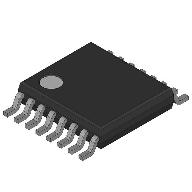
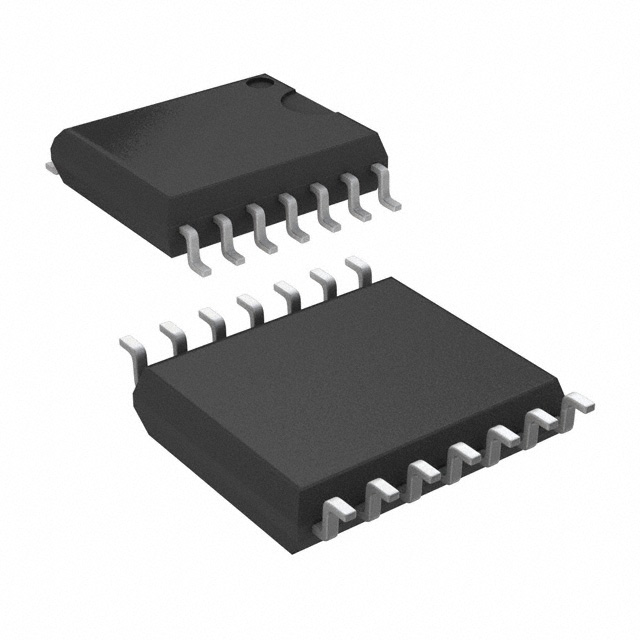
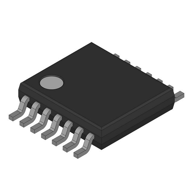
1. Pin Configuration (16-pin TSSOP, Top View)
| Pin # | Function | Description |
|---|---|---|
| 1 | Channel I/O A0 | Analog channel 0 input/output |
| 2 | Channel I/O A1 | Analog channel 1 input/output |
| 3 | Channel I/O A2 | Analog channel 2 input/output |
| 4 | Channel I/O A3 | Analog channel 3 input/output |
| 5 | VEE | Negative supply voltage |
| 6 | GND | Ground |
| 7 | Address SEL S0 | Address select input 0 |
| 8 | Address SEL S1 | Address select input 1 |
| 9 | Address SEL S2 | Address select input 2 |
| 10 | Enable (E) | Active-low enable (High = all switches OFF) |
| 11 | Channel I/O A4 | Analog channel 4 input/output |
| 12 | Channel I/O A5 | Analog channel 5 input/output |
| 13 | Channel I/O A6 | Analog channel 6 input/output |
| 14 | Channel I/O A7 | Analog channel 7 input/output |
| 15 | COM OUT/IN A | Common analog output/input |
| 16 | VCC | Positive supply voltage |
2. Function Table
| Inputs | ON Channel(s) | |||
|---|---|---|---|---|
| E (Enable) | S2 (Address) | S1 (Address) | S0 (Address) | |
| L (Low) | L | L | L | A0 |
| L | L | L | H (High) | A1 |
| L | L | H | L | A2 |
| L | L | H | H | A3 |
| L | H | L | L | A4 |
| L | H | L | H | A5 |
| L | H | H | L | A6 |
| L | H | H | H | A7 |
| H (High) | X (Don’t care) | X | X | None (all switches OFF) |
3. Key Functional Features
- Bidirectional Operation: Any analog channel (A0-A7) can act as input or output, with COM as the common port.
- Break-Before-Make Switching: Prevents signal shorting between channels during switching.
- High Noise Immunity: NIL=30%, NIH=30% of VCC (VCC=5V) for stable digital control.
- Wide Analog Range: Supports analog signals from VEE to VCC (±5V max).
Package and Mechanical Details
1. Package Specifications (16-pin TSSOP/PW)
| Dimension | Min | Nominal | Max | Units |
|---|---|---|---|---|
| Body Length | 4.9 | 5.0 | 5.1 | mm |
| Body Width | 4.3 | 4.5 | 4.55 | mm |
| Package Height | - | - | 1.2 | mm |
| Lead Pitch | 0.65 | 0.65 | - | mm |
| Lead Width | 0.19 | 0.25 | 0.30 | mm |
| Lead Length | 0.50 | 0.65 | 0.75 | mm |
2. Packaging and Shipping
- Tape and Reel: 2000 units per reel (SPQ=2000)
- Reel Dimensions: Diameter=330.0mm, Width (W1)=12.4mm
- Tape Dimensions: Pitch (P1)=8.0mm, Width (W)=12.0mm, Cavity A0=6.9mm, B0=5.6mm, K0=1.6mm
- Pin 1 Orientation: Quadrant Q1 in tape
- Moisture Sensitivity Level (MSL): Level-1-260C-UNLIM
Usage Guidelines and Precautions
- Unused Inputs: All unused control inputs (S0-S2, E) must be tied to VCC or GND to ensure proper operation.
- Supply Considerations: Avoid exceeding 0.6V voltage drop across the switch to prevent VCC current draw; VPP_2V5 must be within 2.3-3.47V during operation.
- Signal Integrity: Keep analog signal paths short to minimize noise; use proper decoupling capacitors near VCC/GND pins.
- Soldering: Follow recommended lead temperature (300°C max for 10s) to avoid package damage.
- Thermal Management: Account for θJA=73°C/W when designing for high-temperature automotive environments.
Purchase
No need to register to order from JMChip Electronics, but signing in lets you track your order like a pro. Give it a try for a smoother shopping ride.
Means
Easy peasy! Pay your way with PayPal, Credit Card, or wire transfer in USD. We've got you covered.
RFQ(Request for Quotations)
Get the freshest prices and stock updates by asking for a quote! Our sales team will shoot you an email within a day. It's that simple.
IMPORTANT NOTICE
1. Look out for your order details in your inbox! (If it's missing, check the spam folder just in case.)
2. Our sales manager will double-check the order and keep you posted on any price or stock changes. No worries, we've got you covered.

Shipping Rate
We ship orders once a day around 5 p.m., except Sunday. Once shipped, the estimated delivery time depends on the courier company you choose, usually 5-7 working days.

Shipping Methods
We provide DHL, FedEx, UPS, EMS, SF Express, and Registered Air Mail international shipping.


Payment
You can pay the orders on the website directly or pay by wire transfer offline. We support: Paypal、VISA、Credit Card.


National Semiconductor
National Semiconductor