
Texas Instruments DS90LV804TSQ/NOPB


- Part Number:
DS90LV804TSQ/NOPB
- Manufacturer:
- Category:
- RoHs:
 RoHS Compliant
 - Datasheet:
 DS90LV804TSQ/NOPB_Datesheet
 - Description:
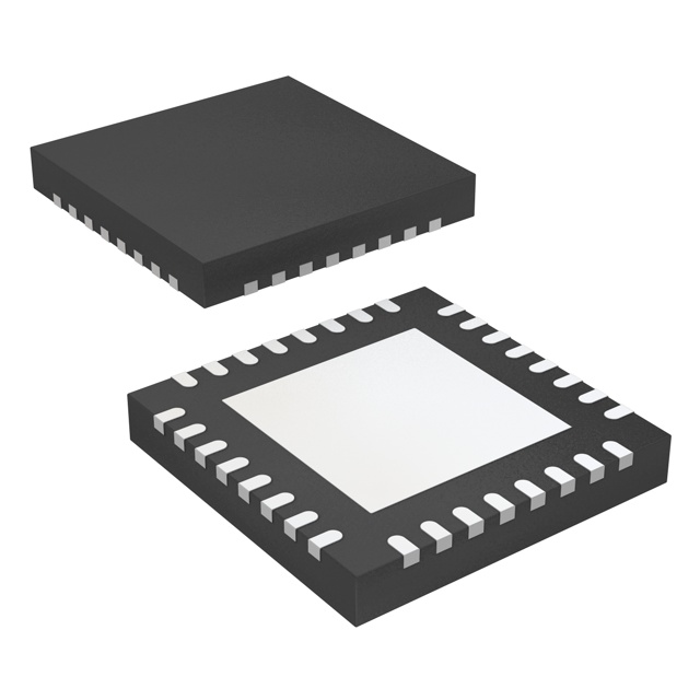
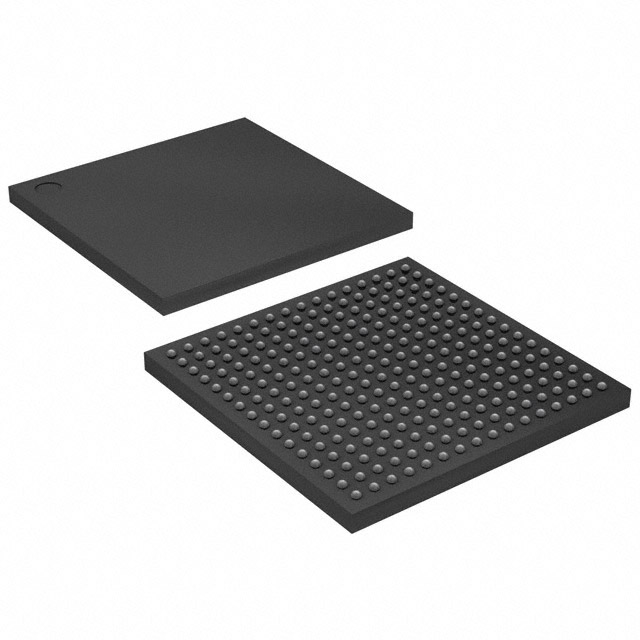
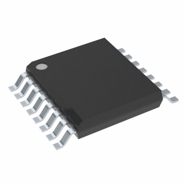
Buffer, ReDriver 4 Channel 800Mbps 32-WQFN (5x5)
- In stock 1,610

DS90LV804TSQ/NOPB Product Information Summary
1. General Description
The DS90LV804TSQ/NOPB is a 4-channel LVDS (Low-Voltage Differential Signaling) buffer/repeater developed by Texas Instruments. It supports a data rate of up to 800 Mbps per channel, featuring on-chip 100Ω input and output terminations to enhance signal integrity. Designed for industrial applications with an operating temperature range of -40°C to +85°C, it comes in a compact WQFN-32 (RTV) leadless package, making it suitable for space-constrained high-speed signal transmission systems such as backplanes and long-distance cable connections.
2. Core Features and Benefits
- High-Speed Data Transmission: Supports 800 Mbps per channel, enabling fast signal repetition and buffering.
- Low Distortion Performance: Minimal output skew (max 80 ps) and jitter (total jitter max 55 psp-p at 800 Mbps) ensure high signal fidelity.
- Multi-Standard Compatibility: Accepts LVDS, CML, and LVPECL differential inputs, with LVDS-compliant outputs for versatile system integration.
- On-Chip Terminations: Integrated 100Ω differential input/output resistors reduce external component count and improve signal integrity.
- Robust ESD Protection: 12 kV HBM ESD protection on LVDS outputs and 8 kV HBM on other pins enhances reliability in harsh environments.
- Low Power Consumption: Typical supply current of 117 mA (active mode) and 2.7 mA (TRI-STATE mode) for energy-efficient operation.
- Industrial Temperature Range: Operates from -40°C to +85°C, suitable for rugged industrial environments.
- Compact Package: WQFN-32 leadless design minimizes PCB footprint and improves thermal performance.
3. Applications
- High-speed backplane signal repetition
- Long-distance cable signal buffering (lossy cable compensation)
- Point-to-point differential signal transmission
- Industrial automation control systems
- LVDS/CML/LVPECL signal conversion and amplification
- Data communication systems requiring low skew and jitter
4. Key Electrical Specifications
4.1 Absolute Maximum Ratings
| Parameter | Conditions | Min | Max | Unit |
|---|---|---|---|---|
| Supply Voltage (VDD) | - | -0.3 | 4.0 | V |
| CMOS Input Voltage (EN) | - | -0.3 | VDD + 0.3 | V |
| LVDS Input Voltage | \(V_{ID(max)} < 2.4 V\) | -0.3 | VDD + 0.3 | V |
| LVDS Output Voltage | - | -0.3 | VDD + 0.3 | V |
| LVDS Output Short Circuit Current | - | - | +90 | mA |
| Junction Temperature | - | - | 150 | °C |
| Storage Temperature | - | -65 | 150 | °C |
| Lead Temperature (Solder, 4 sec) | - | - | 260 | °C |
| Total Package Power Capacity @25°C | - | - | 4.16 | W |
| Thermal Resistance (θJA) | - | - | 29.5 | °C/W |
| Thermal Resistance (θJC) | - | - | 3.5 | °C/W |
| Package Power Derating above 25°C | - | - | 33.3 | mW/°C |
| ESD Protection (LVDS Outputs, HBM) | 1.5 kΩ, 100 pF | - | 12 | kV |
| ESD Protection (Other Pins, HBM) | 1.5 kΩ, 100 pF | - | 8 | kV |
4.2 Recommended Operating Conditions
| Parameter | Conditions | Min | Max | Unit |
|---|---|---|---|---|
| Supply Voltage (VDD) | - | 3.15 | 3.45 | V |
| Input Voltage (VIN) | \(V_{ID(max)} < 2.4 V\) | 0 | VDD | V |
| Output Voltage (VOUT) | - | 0 | VDD | V |
| Operating Temperature (TA) | Industrial Grade | -40 | 85 | °C |
4.3 DC Electrical Characteristics (VDD = 3.3V, TA = 25°C unless stated otherwise)
4.3.1 LVTTL Control Input (EN)
| Symbol | Parameter | Conditions | Min | Typ | Max | Unit |
|---|---|---|---|---|---|---|
| VIH | High-Level Input Voltage | - | 2.0 | - | VDD | V |
| VIL | Low-Level Input Voltage | - | 0 | - | 0.8 | V |
| IIH | High-Level Input Current | VIN = VDD (max) | -10 | - | +10 | µA |
| IIL | Low-Level Input Current | VIN = GND | -10 | - | +10 | µA |
| CIN1 | Input Capacitance | - | - | 3.5 | - | pF |
| VCL | Input Clamp Voltage | ICL = -18 mA | -1.5 | -0.8 | - | V |
4.3.2 LVDS Inputs
| Symbol | Parameter | Conditions | Min | Typ | Max | Unit |
|---|---|---|---|---|---|---|
| VTH | Differential High Threshold | VCM = 0.8–3.4V, VDD = 3.45V | - | 0 | 100 | mV |
| VTL | Differential Low Threshold | VCM = 0.8–3.4V, VDD = 3.45V | -100 | 0 | - | mV |
| VID | Differential Input Voltage | VCM = 0.8–3.4V, VDD = 3.45V | 100 | - | 2400 | mV |
| VCMR | Common-Mode Voltage Range | VID = 150 mV, VDD = 3.45V | 0.05 | - | 3.40 | V |
| CIN2 | Input Capacitance | IN+ or IN- to GND | - | 3.5 | - | pF |
| IIN | Input Current | VIN = 3.45V or 0V | -10 | - | +10 | µA |
4.3.3 LVDS Outputs
| Symbol | Parameter | Conditions | Min | Typ | Max | Unit |
|---|---|---|---|---|---|---|
| VOD | Differential Output Voltage | RL = 100Ω (external) | 250 | 500 | 600 | mV |
| ΔVOD | Change in VOD (Complementary States) | - | -35 | - | 35 | mV |
| VOS | Offset Voltage | - | 1.05 | 1.18 | 1.475 | V |
| ΔVOS | Change in VOS (Complementary States) | - | -35 | - | 35 | mV |
| IOS | Output Short Circuit Current | Short to GND | - | -60 | -90 | mA |
| COUT2 | Output Capacitance (TRI-STATE) | - | - | 5.5 | - | pF |
4.3.4 Supply Current
| Symbol | Parameter | Conditions | Min | Typ | Max | Unit |
|---|---|---|---|---|---|---|
| ICC | Total Supply Current (Active) | All channels enabled, RL = 100Ω | - | 117 | 140 | mA |
| ICCZ | Supply Current (TRI-STATE) | EN = 0V | - | 2.7 | 6 | mA |
4.4 AC Electrical Characteristics (VDD = 3.3V, TA = 25°C)
| Symbol | Parameter | Conditions | Min | Typ | Max | Unit |
|---|---|---|---|---|---|---|
| tLHT | Differential Low-to-High Transition Time | 200 Mbps, 20%–80% VOD | - | 210 | 300 | ps |
| tHLT | Differential High-to-Low Transition Time | 200 Mbps, 20%–80% VOD | - | 210 | 300 | ps |
| tPLHD | Low-to-High Propagation Delay | 200 Mbps, 50% VOD | - | 2.0 | 3.2 | ns |
| tPHLD | High-to-Low Propagation Delay | 200 Mbps, 50% VOD | - | 2.0 | 3.2 | ns |
| tSKD1 | Pulse Skew (tPLHD – tPHLD) | - | - | 25 | 80 | ps |
| tSKCC | Channel-to-Channel Skew | - | - | 50 | 125 | ps |
| tSKP | Part-to-Part Skew | Same temp/VDD | - | - | 1.1 | ns |
| RJ | Random Jitter (RMS) | 400 MHz, alternating 1/0 | - | 1.1 | 1.5 | psrms |
| DJ | Deterministic Jitter (p-p) | 800 Mbps, K28.5 pattern | - | 15 | 35 | psp-p |
| TJ | Total Jitter (p-p) | 800 Mbps, PRBS 2³¹–1 | - | 30 | 55 | psp-p |
| tON | Output Enable Time | EN to active output | - | - | 300 | ns |
| tOFF | Output Disable Time | EN to TRI-STATE | - | - | 12 | ns |
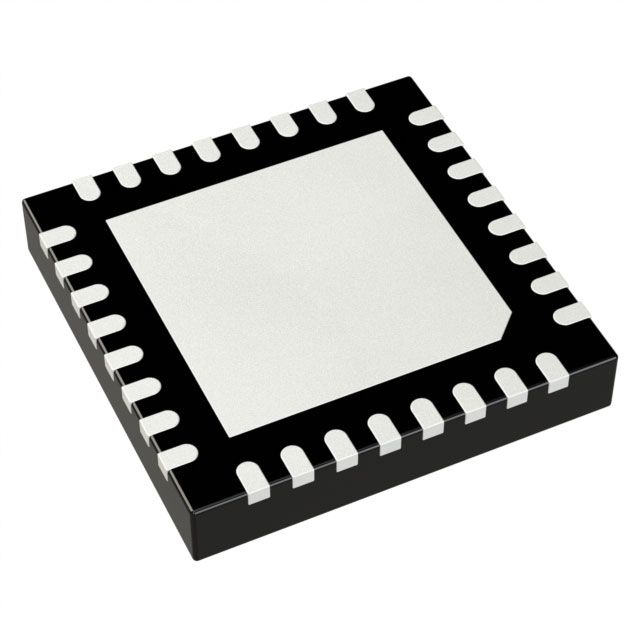
5. Pin Configuration and Description (WQFN-32 Package)
5.1 Pin Layout (Top View)
The device features 32 pins arranged in a WQFN leadless package, with dedicated pins for differential inputs, differential outputs, power, ground, and control.
5.2 Key Pin Descriptions
| Pin Type | Pin Name | Pin Number | I/O Type | Description |
|---|---|---|---|---|
| Differential Inputs | IN0+/IN0- | 9/10 | Input (LVDS) | Channel 0 non-inverting/inverting differential input |
| IN1+/IN1- | 11/12 | Input (LVDS) | Channel 1 non-inverting/inverting differential input | |
| IN2+/IN2- | 13/14 | Input (LVDS) | Channel 2 non-inverting/inverting differential input | |
| IN3+/IN3- | 15/16 | Input (LVDS) | Channel 3 non-inverting/inverting differential input | |
| Differential Outputs | OUT0+/OUT0- | 32/31 | Output (LVDS) | Channel 0 non-inverting/inverting differential output (point-to-point only) |
| OUT1+/OUT1- | 30/29 | Output (LVDS) | Channel 1 non-inverting/inverting differential output (point-to-point only) | |
| OUT2+/OUT2- | 28/27 | Output (LVDS) | Channel 2 non-inverting/inverting differential output (point-to-point only) | |
| OUT3+/OUT3- | 26/25 | Output (LVDS) | Channel 3 non-inverting/inverting differential output (point-to-point only) | |
| Control | EN | 8 | Input (LVTTL) | Enable pin: HIGH = active, LOW = TRI-STATE mode |
| Power | VDD | 3,4,6,7,19,20,21,22 | Power | 3.3V supply (±5% tolerance) |
| Ground | GND | 1,2,5,17,18 | Power | Ground reference (DAP (exposed pad) must be connected to GND for thermal/AC performance) |
| No Connect | N/C | 23,24 | - | Unused pins (leave open) Note: The exposed DAP (Die Attach Pad) on the WQFN package is the primary GND connection and must be soldered to the PCB ground plane with at least 4 vias. |
6. Package and Mechanical Specifications
6.1 Package Details
| Parameter | Value |
|---|---|
| Package Type | WQFN-32 (RTV) |
| Package Category | Leadless Leadframe Package (LLP) |
| Pin Count | 32 |
| Package Dimensions (Length × Width × Height) | 5.3 mm × 5.3 mm × 0.8 mm (max) |
| Exposed Pad (DAP) | Required for grounding and thermal dissipation |
| Moisture Sensitivity Level (MSL) | Level 3 (260°C peak reflow, 168 hours floor life) |
| Lead Finish | Tin (SN) |
| RoHS Compliance | Yes |
6.2 Tape and Reel Specifications
| Parameter | Value |
|---|---|
| Reel Diameter | 177.8 mm (7 inches) |
| Reel Width (W1) | 12.4 mm |
| Tape Pitch (P1) | 8.0 mm |
| Component Orientation (Pin1 Quadrant) | Q1 |
| Quantity per Reel (SPQ) | 1000 units |
7. Functional Operation
7.1 Active Mode
When EN is HIGH, the device amplifies and repeats differential input signals to the LVDS outputs. On-chip 100Ω terminations minimize signal reflections, ensuring high integrity for high-speed data.
7.2 TRI-STATE Mode
When EN is LOW, all input/output buffers and internal bias circuits are disabled. Outputs enter a high-impedance state, reducing power consumption to typical 2.7 mA. A 300 ns enable delay and 12 ns disable delay apply when switching modes.
7.3 Input Failsafe Biasing
For open-circuit input conditions, use 5kΩ–15kΩ pull-up (IN+ to VDD) and pull-down (IN- to GND) resistors. Set the common-mode bias to ~1.2V (≤1.75V) for compatibility with internal circuitry (refer to AN-1194 for details).
7.4 Input/Output Interfacing
- Inputs: DC-coupled to LVDS/CML/LVPECL drivers (internal 100Ω termination eliminates external resistors).
- Outputs: DC-coupled to LVDS/CML/LVPECL receivers (optimized for point-to-point, not multidrop applications).
8. Application Notes
- PCB Layout: Connect the DAP to the ground plane with multiple vias for thermal and AC performance. Keep differential trace lengths matched to minimize skew.
- Termination: Internal 100Ω terminations are included; no external resistors are required for differential pairs.
- ESD Protection: Store/handle with leads shorted or in conductive foam to prevent MOS gate damage.
- Power Supply: Decouple VDD pins with 0.1µF ceramic capacitors placed close to each pin for noise suppression.
9. Ordering Information
| Orderable Part Number | DS90LV804TSQ/NOPB |
|---|---|
| Status | Active |
| Material Type | Production |
| Operating Temperature Range | -40°C to +85°C |
| Part Marking | 804TSQ |
| RoHS Compliance | Yes |
Purchase
No need to register to order from JMChip Electronics, but signing in lets you track your order like a pro. Give it a try for a smoother shopping ride.
Means
Easy peasy! Pay your way with PayPal, Credit Card, or wire transfer in USD. We've got you covered.
RFQ(Request for Quotations)
Get the freshest prices and stock updates by asking for a quote! Our sales team will shoot you an email within a day. It's that simple.
IMPORTANT NOTICE
1. Look out for your order details in your inbox! (If it's missing, check the spam folder just in case.)
2. Our sales manager will double-check the order and keep you posted on any price or stock changes. No worries, we've got you covered.

Shipping Rate
We ship orders once a day around 5 p.m., except Sunday. Once shipped, the estimated delivery time depends on the courier company you choose, usually 5-7 working days.

Shipping Methods
We provide DHL, FedEx, UPS, EMS, SF Express, and Registered Air Mail international shipping.


Payment
You can pay the orders on the website directly or pay by wire transfer offline. We support: Paypal、VISA、Credit Card.


Texas Instruments
Texas Instruments
Texas Instruments
Texas Instruments
Texas Instruments
Texas Instruments
Texas Instruments

Texas Instruments
Texas Instruments
Texas Instruments
Texas Instruments

Texas Instruments