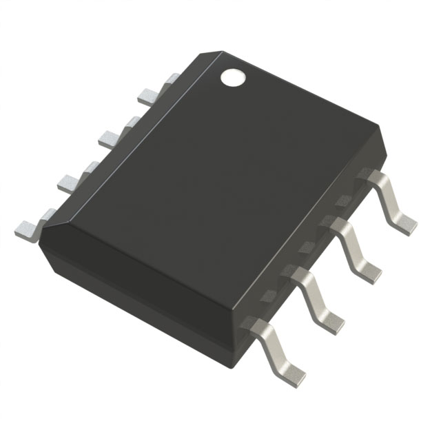
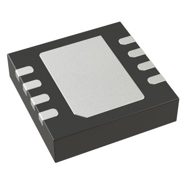
Rochester Sensors EP900DM/B


- Part Number:
EP900DM/B
- Manufacturer:
- Category:
- RoHs:
 Non-RoHS Compliant
 - Datasheet:
- Description:
EP900DM/B
- In stock 1,200
EP900DM/B Classic EPLD Specification Sheet
1. General Description
The EP900DM/B belongs to Altera’s Classic EPLD (Erasable Programmable Logic Device) family, manufactured by Rochester Electronics. It is designed for high-speed, low-power logic integration, leveraging advanced CMOS technology to support 100% TTL emulation. This device integrates multiple PAL- and GAL-type logic functions, offering a balance of logic density, speed, and flexibility for industrial, military, and space-grade applications. It features non-volatile EPROM configuration elements, enabling erasure and reprogramming, and supports a wide range of packages for versatile system integration.
2. Key Features
- Logic Density: Estimated 450 usable gates (aligning with the EP910 variant in the Classic family)
- Macrocells: 24 programmable macrocells, configurable for sequential (D, T, JK, SR flipflops) or combinatorial operation
- I/O Capabilities: Up to 38 maximum user I/O pins, with programmable I/O architecture
- Performance:
- Programmability:
- Clock Flexibility: Dual global clock pins (CLK1, CLK2) and array clock capability for independent register clocking
- Software & Hardware Support: Compatible with Altera MAX+PLUS II development system; programmable via Altera MPU, Data I/O, and third-party programmers
- Quality & Reliability:
3. Package Information
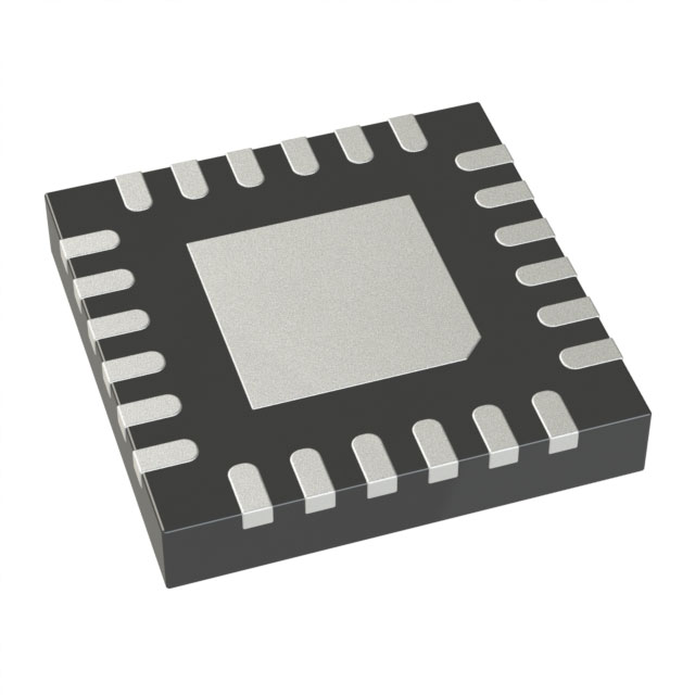
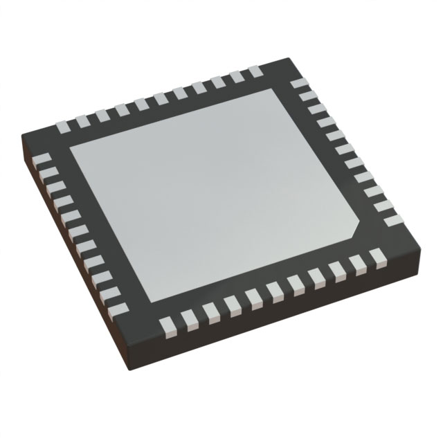
- Package Types: Compatible with the Classic family’s EP910 variant packages, including:
- Lead Finish: RoHS-compliant (Pb-free) options available (per Rochester’s manufacturing standards)
- Temperature Range: Industrial (-40°C to 85°C) and commercial (0°C to 70°C) grades supported
- Storage Temperature: -65°C to 150°C (no bias)
4. Functional Architecture
4.1 Core Components
- Macrocells: 24 macrocells, each with 8 product terms (programmable-AND/fixed-OR structure) and an XOR gate for polarity control. Supports asynchronous clear via a dedicated product term.
- Programmable Registers: Individually configurable as D, T, JK, or SR flipflops, or bypassed for combinatorial logic. Automatically cleared on power-up.
- Clock & Output Control: Two operating modes for output enable/clock select:
- Feedback Select: Global feedback configuration (similar to EP910), allowing macrocell outputs or I/O pin inputs to feed back to the AND array, accessible to all macrocells.
4.2 Block Diagram Overview
plaintext
[Dedicated Inputs / I/O Pins] → [Global Bus (True/Complement Signals)] → [Programmable-AND Array] → [OR Gate] → [XOR Gate] → [Programmable Register / Combinatorial Path] → [Tri-State Output Buffer] → [I/O Pins]
                                                                 ↑                                  ↑
                                                         [Feedback Multiplexer]                [Clock/Output Enable Select]
                                                                 ↑                                  ↑
                                                         [Macrocell/I/O Feedback]             [Global Clock / Array Clock]
5. Electrical Characteristics
5.1 Absolute Maximum Ratings
| Parameter | Conditions | Min | Max | Unit |
|---|---|---|---|---|
| VCC | Supply voltage (with respect to ground) | -2.0 | 7.0 | V |
| VI | DC input voltage | -2.0 (EP910) / -0.5 (EP910I) | 7.0 (EP910) / VCC+0.5 (EP910I) | V |
| IMAX | DC VCC or ground current | -250 | 250 | mA |
| IOUT | DC output current (per pin) | -25 | 25 | mA |
| TSTG | Storage temperature (no bias) | -65 | 150 | °C |
| TAMB | Ambient temperature (under bias) | -65 | 135 | °C |
| TJ | Junction temperature (ceramic packages, under bias) | - | 150 | °C |
| TJ | Junction temperature (plastic packages, under bias) | - | 135 | °C |
5.2 Recommended Operating Conditions
| Parameter | Conditions | Min | Max | Unit |
|---|---|---|---|---|
| VCC | Supply voltage (commercial) | 4.75 | 5.25 | V |
| VCC | Supply voltage (industrial) | 4.5 | 5.5 | V |
| VI | Input voltage | -0.3 | VCC+0.3 | V |
| VO | Output voltage | 0 | VCC | V |
| TA | Operating temperature (commercial) | 0 | 70 | °C |
| TA | Operating temperature (industrial) | -40 | 85 | °C |
| tR / tF | Input rise/fall time (commercial) | - | 100 | ns |
| tR / tF | Input rise/fall time (industrial) | - | 50 | ns |
5.3 DC Electrical Characteristics (VCC = 5V ±5%, TA = 25°C)
| Parameter | Conditions | Min | Max | Unit |
|---|---|---|---|---|
| VIH | High-level input voltage | 2.0 | VCC+0.3 | V |
| VIL | Low-level input voltage | -0.3 | 0.8 | V |
| VOH (TTL) | High-level output voltage (IOH = -4 mA) | 2.4 | - | V |
| VOH (CMOS) | High-level output voltage (IOH = -0.6 mA) | 3.84 | - | V |
| VOL | Low-level output voltage (IOL = 4 mA) | - | 0.45 | V |
| II | I/O pin leakage current (dedicated inputs) | -10 | 10 | μA |
| IOZ | Tri-state output leakage current | -10 | 10 | μA |
5.4 Supply Current (ICC)
| Parameter | Conditions | Typ | Max | Unit |
|---|---|---|---|---|
| ICC1 (Non-Turbo, Standby) | No load, no logic transitions | 20 (EP910) / 60 (EP910I) | 150 | μA |
| ICC2 (Non-Turbo, Active) | No load, f = 1 MHz | 6 (EP910) / 4 (EP910I) | 20 (EP910) / 12 (EP910I) | mA |
| ICC3 (Turbo, Active) | No load, f = 1 MHz | 45 (EP910) / 120 (EP910I) | 80 (100) (EP910) / 150 (EP910I) | mA |
5.5 Capacitance (TA = 25°C, f = 1 MHz)
| Parameter | Conditions | Max | Unit |
|---|---|---|---|
| CIN | Input pin capacitance | 20 (EP910) / 8 (EP910I) | pF |
| CIO | I/O pin capacitance | 20 (EP910) / 8 (EP910I) | pF |
| CCLK1 | CLK1 pin capacitance | 20 (EP910) / 10 (EP910I) | pF |
| CCLK2 | CLK2 pin capacitance | 60 (EP910) / 12 (EP910I) | pF |
6. Timing Parameters (Turbo Mode Enabled)
6.1 External Timing Parameters (EP910I-12 Variant Reference)
| Parameter | Conditions | Min | Max | Unit |
|---|---|---|---|---|
| tPD1 | Input to non-registered output (C1 = 35 pF) | - | 12.0 | ns |
| tPD2 | I/O input to non-registered output (C1 = 35 pF) | - | 12.0 | ns |
| tPZX | Input to output enable (C1 = 35 pF) | - | 15.0 | ns |
| tPXZ | Input to output disable (C1 = 5 pF) | - | 15.0 | ns |
| tCLR | Asynchronous output clear time (C1 = 35 pF) | - | 15.0 | ns |
| fMAX | Maximum pipelined frequency | 125.0 | - | MHz |
| tSU (Global) | Global clock setup time | 8.0 | - | ns |
| tH (Global) | Global clock hold time | 0.0 | - | ns |
| tCH | Global clock high time | 5.0 | - | ns |
| tCL | Global clock low time | 5.0 | - | ns |
| tCO1 | Global clock to output delay (C1 = 35 pF) | - | 8.0 | ns |
| tCNT | Global clock minimum period | - | 13.0 | ns |
| fCNT | Maximum internal global clock frequency | 76.9 | - | MHz |
6.2 Internal Timing Parameters (EP910I-12 Variant Reference)
| Parameter | Conditions | Max | Unit |
|---|---|---|---|
| tIN | Input pad and buffer delay | 2.0 | ns |
| tIO | I/O input pad and buffer delay | 0.0 | ns |
| tLAD | Logic array delay | 8.0 | ns |
| tOD | Output buffer and pad delay (C1 = 35 pF) | 2.0 | ns |
| tZX | Output buffer enable delay (C1 = 35 pF) | 5.0 | ns |
| tXZ | Output buffer disable delay (C1 = 5 pF) | 5.0 | ns |
| tSU (Register) | Register setup time | 4.0 | ns |
| tH (Register) | Register hold time | 4.0 | ns |
| tIC | Array clock delay | 12.0 | ns |
| tICS | Global clock delay | 4.0 | ns |
| tFD | Feedback delay | 1.0 | ns |
| tCLR (Register) | Register clear time | 11.0 | ns |
7. Programming & Design Support
7.1 Programming
- Erasure: UV light erasure (windowed ceramic packages) for design modifications.
- Programming Tools: Altera Master Programming Unit (MPU), Data I/O, BP Microsystems, and third-party programmers.
- Security: Programmable security bit to prevent design copying; reset only via UV erasure.
7.2 Software Support
- Development System: Altera MAX+PLUS II (runs on Windows PCs, Sun SPARCstation, HP 9000, IBM RISC System/6000).
- Design Entry: Schematic, VHDL, Verilog HDL, AHDL, EDIF, and LPM interfaces.
- Simulation & Timing: Integrated timing analysis, simulation, and point-to-point delay prediction.
Purchase
No need to register to order from JMChip Electronics, but signing in lets you track your order like a pro. Give it a try for a smoother shopping ride.
Means
Easy peasy! Pay your way with PayPal, Credit Card, or wire transfer in USD. We've got you covered.
RFQ(Request for Quotations)
Get the freshest prices and stock updates by asking for a quote! Our sales team will shoot you an email within a day. It's that simple.
IMPORTANT NOTICE
1. Look out for your order details in your inbox! (If it's missing, check the spam folder just in case.)
2. Our sales manager will double-check the order and keep you posted on any price or stock changes. No worries, we've got you covered.

Shipping Rate
We ship orders once a day around 5 p.m., except Sunday. Once shipped, the estimated delivery time depends on the courier company you choose, usually 5-7 working days.

Shipping Methods
We provide DHL, FedEx, UPS, EMS, SF Express, and Registered Air Mail international shipping.


Payment
You can pay the orders on the website directly or pay by wire transfer offline. We support: Paypal、VISA、Credit Card.


