Nisshinbo Micro Devices Inc. NJW4301M


- Part Number:
NJW4301M
- Manufacturer:
- Category:
- RoHs:
 Non-RoHS Compliant
 - Datasheet:
 NJW4301M_Datesheet
 - Description:
IC HALF BRIDGE DRIVER 30SDMP
- In stock 0

NJW4301M Datasheet Summary
General Description
The NJW4301M is a 2-channel bridge driver IC designed for applications such as CD, CD-ROM, and MO devices. It operates at a supply voltage of 4V to 12V and features high output voltage swing. The output circuit is composed of MOS-FETs, which offer lower power consumption compared to bipolar outputs, simplifying thermal design and reducing overall costs.
Package Outline
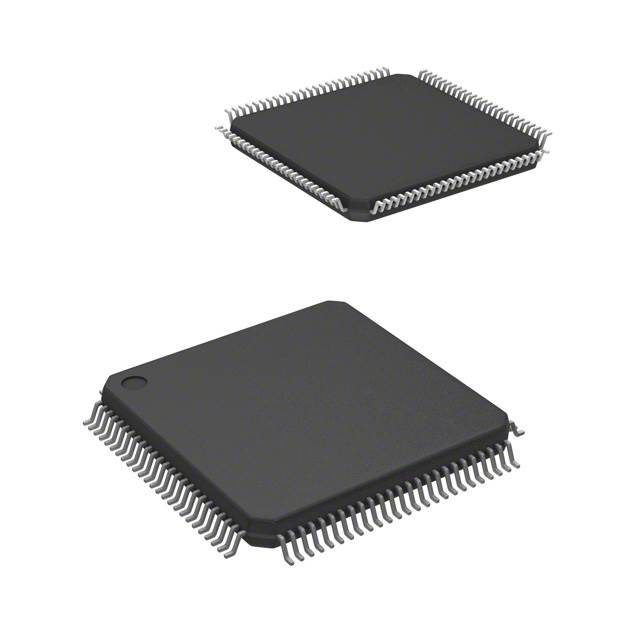
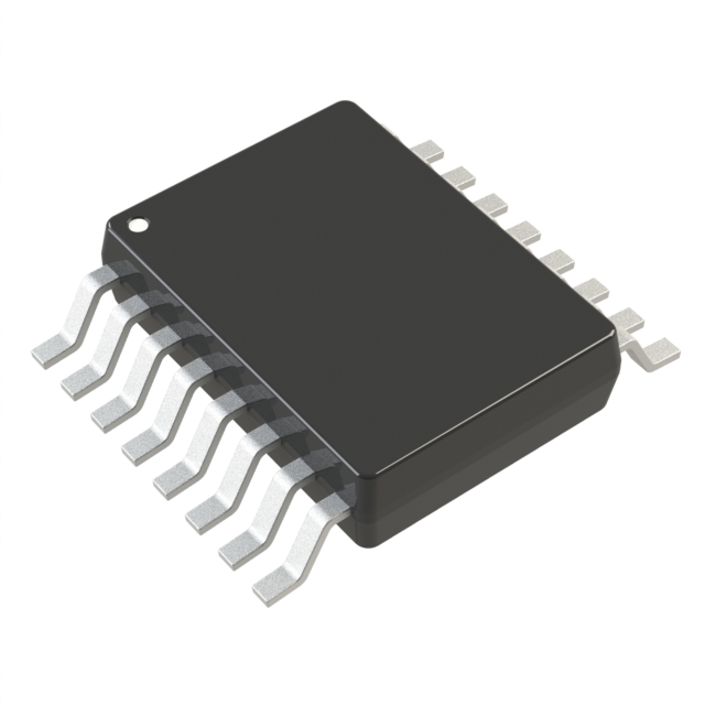
- Package Type: DIP-16, SDMP-30
Features
- Operating Voltage: V+ = 4V to 12V
- Low Saturation Output: Vsat = ±0.5V MAX at IO = 300mA
- Supply Current: 35mA MAX
- 2-channel BTL Output
- Mute Function
- Bi-MOS Technology
Absolute Maximum Ratings (Ta = 25°C)
- Supply Voltage (V+): 15V
- Operating Current (IO): 1A
- Mute Terminal Current (IM): 1.0mA
- Power Dissipation (PD): 1.9W (DIP16), 1.8W (SDMP30) (Note: At 1 PC board)
- Operating Temperature Range: -40°C to +85°C
- Storage Temperature Range: -40°C to +150°C
Electrical Characteristics (V+ = 5V, Ta = 25°C)
- Operating Supply Voltage Range: 4V to 12V
- Mute OFF Current Dissipation (ICC1): 0.5mA to 35mA
- Mute ON Current Dissipation (ICC2): 2mA to 3.5mA
- Output Offset Voltage (VOF): ±50mV (OUT1-OUT2, OUT4-OUT3, GAIN=1)
- Input Common Mode Voltage Range (VICM): 0V to V+ (AMP2, AMP3)
- Input Bias Current (IB): 300nA MAX
- Maximum Output Voltage (VO1, VO2): 4.0V to 4.2V at 300mA, 3.0V to 3.5V at 500mA
- Open Loop Voltage Gain (AV): 35dB to 50dB (AMP2, AMP3, R=2KΩ, VIN=2.5V)
- Input Output Potential Difference (VBIO): ±30mV
- Input Voltage Range (VBICM): 1.5V to 3.5V
- Output Voltage Range (ΔVBO): -50mV to +50mV (VIN=2.5V, IL=-5mA to +5mA)
- Mute OFF Voltage (VOFF): 3.5V to 4.2V
- Mute ON Voltage (VON): 0.8V to 1.0V
- Mute Sink Current (IM): 70µA to 130µA
Pin Configuration
DIP-16
- V+: Supply Voltage
- MUTE: Mute Control
- OUT1: Output Terminal of AMP.1
- GND: Ground
- GND: Ground
- OUT2: Output Terminal of AMP.2
- Vin1(-): Inverting Input of AMP.2
- Vin1(+): Non-Inverting Input of AMP.2
- Vin2(+): Inverting Input of AMP.3
- Vin2(-): Non-Inverting Input of AMP.3
- OUT3: Output Terminal of AMP.3
- GND: Ground
- GND: Ground
- OUT4: Output Terminal of AMP.4
- Vbout: Buffer Output
- VBin: Buffer Input
SDMP-30
- GND: Ground
- GND: Ground
- OUT4: Output Terminal of AMP.4
- NC: Non-Connection
- NC: Non-Connection
- VBout: Buffer Output
- VBin: Buffer Input
- NC: Non-Connection
- V+: Supply Voltage
- MUTE: Mute Control
- NC: Non-Connection
- NC: Non-Connection
- OUT1: Output Terminal of AMP.1
- GND: Ground
- GND: Ground
- GND: Ground
- GND: Ground
- OUT2: Output Terminal of AMP.2
- NC: Non-Connection
- NC: Non-Connection
- Vin1(-): Inverting Input of AMP.2
- Vin1(+): Non-Inverting Input of AMP.2
- NC: Non-Connection
- Vin2(+): Inverting Input of AMP.3
- Vin2(-): Non-Inverting Input of AMP.3
- NC: Non-Connection
- NC: Non-Connection
- OUT3: Output Terminal of AMP.3
- GND: Ground
- GND: Ground
Terminal Explanation
- GND: Ground terminal, recommended for expanding the island to improve heat radiation properties.
- OUT1, OUT2, OUT3, OUT4: Output terminals of the amplifiers, with OUT1 and OUT2, OUT3 and OUT4 being opposite phase.
- VBin, Vbout: Buffer input and output terminals.
- V+: Supply voltage terminal.
- MUTE: Mute control terminal with a pulldown resistor.
- Vin1(-), Vin1(+), Vin2(-), Vin2(+): Input terminals for the amplifiers.
Application Circuits
The datasheet provides application circuits for both DIP-16 and SDMP-30 packages, showing how to connect the NJW4301M in typical configurations for driving speakers or other loads.
Typical Characteristics
The datasheet includes graphs and charts detailing the typical performance characteristics of the NJW4301M, such as output offset voltage vs. operating voltage, operating current vs. operating voltage, output voltage range vs. output current, total harmonic distortion vs. output power, and total harmonic distortion vs. frequency.
Caution
The specifications provided in this datasheet are for informational purposes only and do not guarantee the absence of errors or omissions. The application circuits are illustrative and do not constitute a guarantee or permission for any rights, including industrial rights.
Purchase
No need to register to order from JMChip Electronics, but signing in lets you track your order like a pro. Give it a try for a smoother shopping ride.
Means
Easy peasy! Pay your way with PayPal, Credit Card, or wire transfer in USD. We've got you covered.
RFQ(Request for Quotations)
Get the freshest prices and stock updates by asking for a quote! Our sales team will shoot you an email within a day. It's that simple.
IMPORTANT NOTICE
1. Look out for your order details in your inbox! (If it's missing, check the spam folder just in case.)
2. Our sales manager will double-check the order and keep you posted on any price or stock changes. No worries, we've got you covered.

Shipping Rate
We ship orders once a day around 5 p.m., except Sunday. Once shipped, the estimated delivery time depends on the courier company you choose, usually 5-7 working days.

Shipping Methods
We provide DHL, FedEx, UPS, EMS, SF Express, and Registered Air Mail international shipping.


Payment
You can pay the orders on the website directly or pay by wire transfer offline. We support: Paypal、VISA、Credit Card.