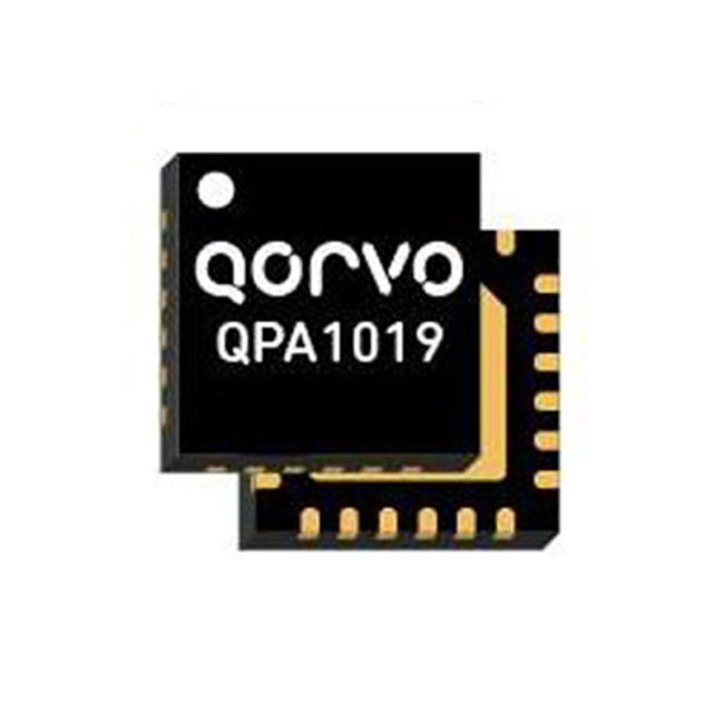
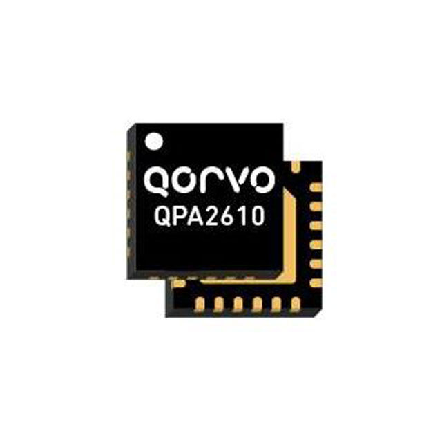
Qorvo QPA2610


- Part Number:
QPA2610
- Manufacturer:
- Category:
- RoHs:
 RoHS Compliant
 - Datasheet:
 QPA2610_Datesheet
 - Description:
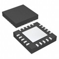
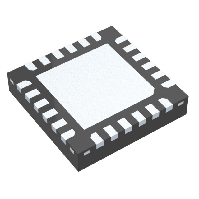
RF Amplifier IC General Purpose 8.5GHz ~ 10.5GHz 24-QFN (5x5)
- In stock 100

QPA2610 Model Information
Model Overview
- Model Number: QPA2610
- Frequency Range: 8.5 – 10.5 GHz
- Package Type: 5 mm x 5 mm plastic overmold QFN
- Operating Temperature Range: -40°C to +85°C
- Storage Temperature Range: -55°C to +100°C
- Key Features
- Output Power (PIN = 10 dBm): > 33 dBm
- Power Added Efficiency (PAE) (PIN = 10 dBm): > 47%
- Small Signal Gain: > 37.5 dB
- Input Return Loss: > 14 dB
- Output Return Loss: > 12 dB
- Recommended Bias: VD = 20 V, IDQ = 56 mA
- Package Size: 5.0 mm x 5.0 mm x 0.85 mm
- Lead-free and RoHS Compliant
- Product Overview
Qorvo's QPA2610 is a high-performance power amplifier designed for X-Band applications. Fabricated on Qorvo's production 0.15 um GaN on SiC process (QGaN15), the QPA2610 delivers > 2 W of saturated output power and 23 dB of large-signal gain while achieving an impressive 47% power-added efficiency. The amplifier is packaged in a compact 5 x 5 mm plastic overmold QFN, making it suitable for phased array radar applications. The RF input and output ports are matched to 50 Ω and include integrated DC blocking capacitors. The QPA2610 is part of a three-amplifier family and is pin-compatible with QPA2612 and QPA2611. - Ordering Information
- Part No.: QPA2610
- Description: 2 Watt X-Band Power Amplifier
- Part No.: QPA2610TR7
- Description: 500 pcs. on 7 inch reel
- Part No.: QPA2610EVB
- Description: QPA2610 Evaluation Board
- Applications
- Radar: Suitable for radar systems requiring high power and efficiency
- Communications: Ideal for high-frequency communication systems
- Satcom: Suitable for satellite communication applications
- Electrical Specifications
- Operational Frequency: 8.5 – 10.5 GHz
- Output Power (PIN = 10 dBm): > 33.9 dBm
- Power Added Efficiency (PIN = 10 dBm): > 47.4%
- Small Signal Gain (CW): > 38.5 dB
- Input Return Loss (CW): > 19 dB
- Output Return Loss (CW): > 14 dB
- 3rd Order IMD (PIN/Tone = 0 dBm): -15 dBc at 10 MHz tone spacing
- POUT Temp. Coeff. (85°C to 25°C, PIN = 10 dBm): -0.21 dB/°C
- Small Signal Gain Temp. Coefficient (85°C to -40°C): -0.09 dB/°C
- Gate Leakage Current (VD = 10 V, VG = -3.7 V): -1.23 mA
- Absolute Maximum Ratings
- Drain Voltage (VD): 29.5 V
- Gate Voltage Range (VG): -4 to 0 V
- Drain Current (ID): 700 mA
- Gate Current (IG): See plot on page 16
- Power Dissipation (PDISS), TBASE = 85 °C: 8.8 W
- Input Power (PIN), Pulsed (100us/10%), 50 Ω, VD = 20 V, TBASE = 85 °C: 18 dBm
- Input Power (PIN), Pulsed (100us/10%), VSWR 3:1, VD = 20 V, TBASE = 85 °C: 18 dBm
- Mounting Temperature (30 seconds max.): 260 °C
- Storage Temperature: -55 to 150 °C
- Performance Plots
- Output Power vs. Frequency: Varies with frequency and temperature, see charts for detailed data.
- Power Added Efficiency vs. Frequency: Varies with frequency and temperature, see charts for detailed data.
- Drain Current vs. Frequency: Varies with frequency and temperature, see charts for detailed data.
- Gate Current vs. Frequency: Varies with frequency and temperature, see charts for detailed data.
- Output Power vs. Input Power: Varies with input power and frequency, see charts for detailed data.
- Power Added Efficiency vs. Input Power: Varies with input power and frequency, see charts for detailed data.
- Drain Current vs. Input Power: Varies with input power and frequency, see charts for detailed data.
- Gate Current vs. Input Power: Varies with input power and frequency, see charts for detailed data.
- Thermal and Reliability Information
- Thermal Resistance (θJC): 11.30 °C/W (Tbase = +85 °C, VD = 20 V, IDQ = 56 mA, PDISS = 1.12 W)
- Channel Temperature (TCH): 97.7 °C (under RF conditions)
- Bias-up and Bias-down Procedure
- Bias-up: Set ID limit to 750 mA, IG limit to 10 mA. Apply -4 V to VG, then +20 V to VD. Adjust VG until IDQ = 56 mA.
- Bias-down: Turn off RF signal. Reduce VG to -4 V, then set VD to 0 V. Turn off VD and VG supplies.
- Mechanical Information
- Package Base and Leads: Ni-Au plated
- Part Markings: QPA2610, Assembly Year, Assembly Week, Lot Number
- Handling Precautions
- ESD-Sensitive Device: Handle with care to avoid ESD damage.
- Moisture Sensitivity Level (MSL): Level 3
- RoHS Compliance: Compliant with 2011/65/EU RoHS directive
Purchase
No need to register to order from JMChip Electronics, but signing in lets you track your order like a pro. Give it a try for a smoother shopping ride.
Means
Easy peasy! Pay your way with PayPal, Credit Card, or wire transfer in USD. We've got you covered.
RFQ(Request for Quotations)
Get the freshest prices and stock updates by asking for a quote! Our sales team will shoot you an email within a day. It's that simple.
IMPORTANT NOTICE
1. Look out for your order details in your inbox! (If it's missing, check the spam folder just in case.)
2. Our sales manager will double-check the order and keep you posted on any price or stock changes. No worries, we've got you covered.

Shipping Rate
We ship orders once a day around 5 p.m., except Sunday. Once shipped, the estimated delivery time depends on the courier company you choose, usually 5-7 working days.

Shipping Methods
We provide DHL, FedEx, UPS, EMS, SF Express, and Registered Air Mail international shipping.


Payment
You can pay the orders on the website directly or pay by wire transfer offline. We support: Paypal、VISA、Credit Card.