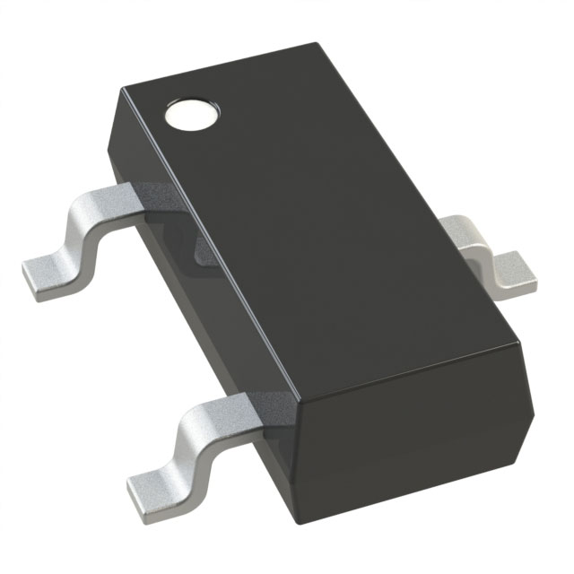
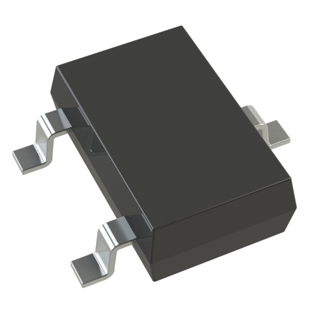
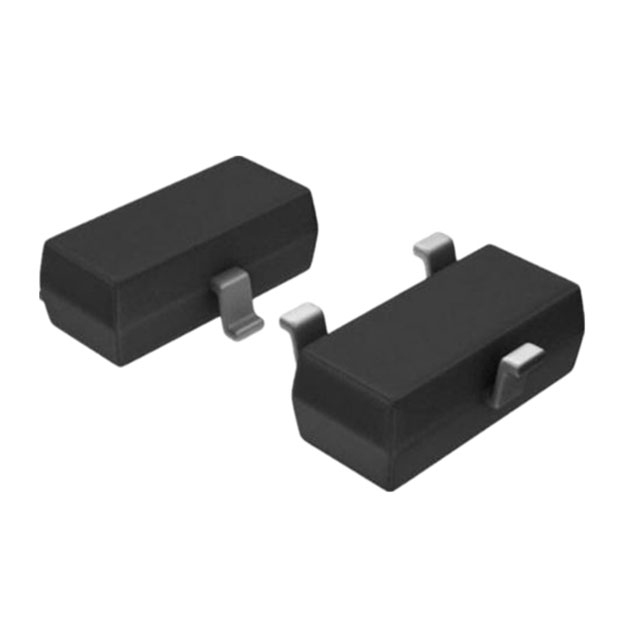
MDD 2N7002K


- Part Number:
2N7002K
- Manufacturer:
- Category:
- RoHs:
 RoHS Compliant
 - Datasheet:
 2N7002K_Datesheet
 - Description:
MOSFET SOT-23 N Channel 60V
- In stock 786,000

Specification Sheet for SOT232N70S702K MOSFET
Basic Information
- Part Number: SOT232N70S702K
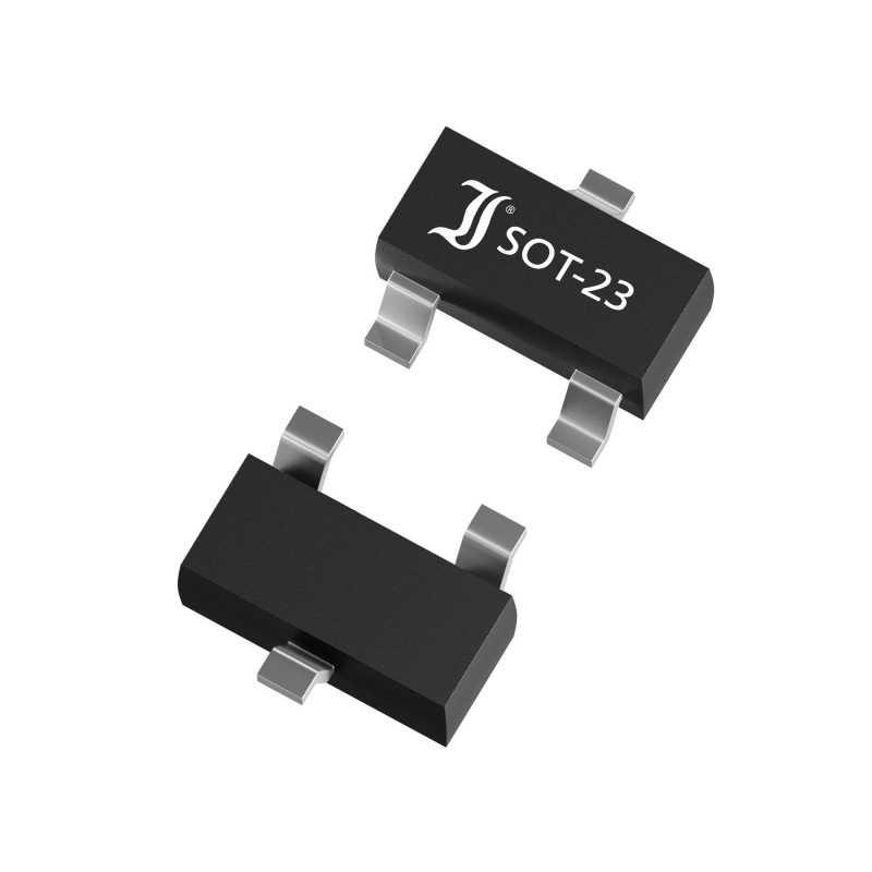
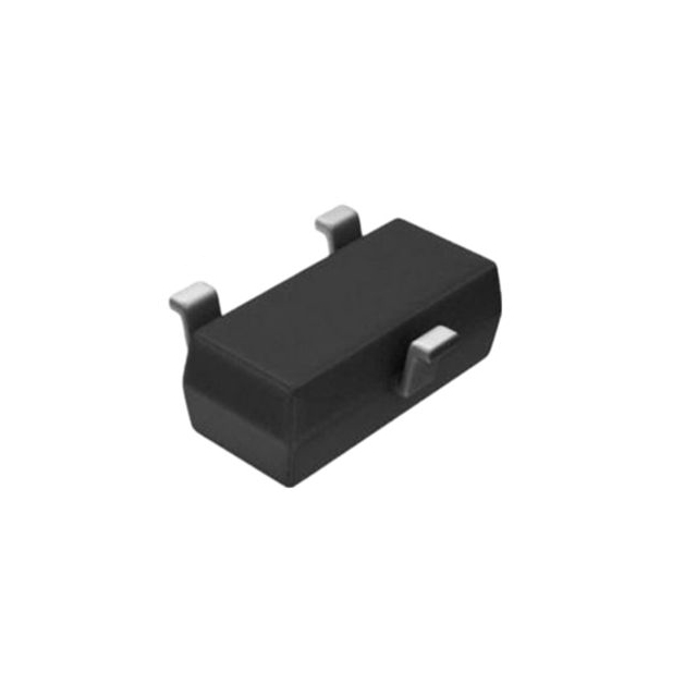
- Description: SMD Plastic-Encapsulate MOSFETs, SOT-23 series, 3 pads
- Type: 2N7002K Type, 60V N-Channel Enhancement Mode MOSFET
- Vendor: NextGen Components, Inc.
- Compliance: RoHS/RoHS III compliant
- Package: Tape/Reel, 3000pcs/Reel
Main Features
- High density cell design for low RDS(ON)
- Voltage controlled small signal switch
- Rugged and reliable
- High saturation current capability
- HMB ESD protected (2000V)
Applications
- Load Switch for Portable Devices
- DC/DC Converter
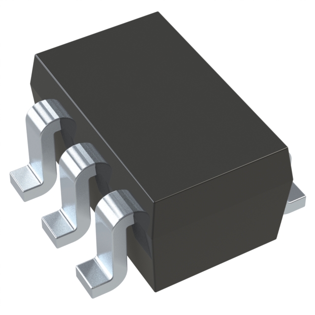
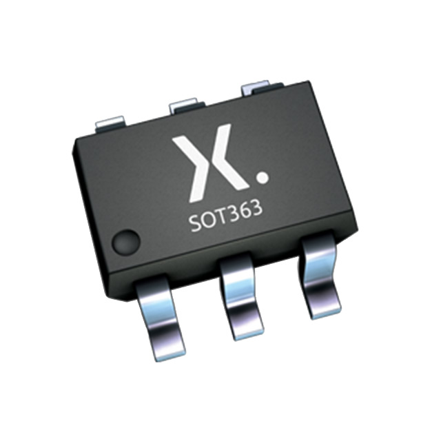
Package and Marking
- Package Code: SOT23
- Marking Code: 702K
- Dimensions:A: 1.0 - 1.4 mmA1: 0.10 mmb: 0.35 - 0.50 mmc: 0.10 - 0.20 mmD: 2.70 - 3.10 mmE: 1.40 - 1.60 mmE1: 2.40 - 2.80 mme: 1.9 mmL: 0.10 - 0.30 mmL1: 0.40 mmƟ: 0° - 10°
Electrical Characteristics (Ta=25°C unless otherwise specified)
Max. Ratings
- Drain-Source Voltage (VDS): 60V
- Gate-Source Voltage (VGS): ±20V
- Continuous Drain Current (ID): 0.6A
- Power Dissipation (PD): 0.3W
- Thermal Resistance (RθJA): 400°C/W
- Junction Temperature (TJ): +150°C
- Storage Temperature Range (TSTG): -50°C to +150°C
MOSFET Electrical Characteristics
- Drain-Source Breakdown Voltage (V(BR)DSS): 60V (VGS=0V, ID=250μA)
- Zero Gate Voltage Drain Current (IDSS): 1µA (VDS=60V, VGS=0V) at 25°C, 100µA at 125°C
- Gate-Body Leakage Current (IGSS): ±10µA (VGS=±20V, VDS=0V)
- Gate Threshold Voltage (VGS(TH)): 1.0 - 2.5V (VDS=VGS, ID=250μA)
- Drain-Source On-State Resistance (RDS(ON)):0.9Ω @ VGS=10V, ID=0.5A1.4Ω @ VGS=4.5V, ID=0.3A
Dynamic Electrical Characteristics
- Input Capacitance (Ciss): 23.8pF (VDS=30V, VGS=0V, f=1MHz)
- Output Capacitance (Coss): 3.9pF
- Reverse Transfer Capacitance (Crss): 1.5pF
- Total Gate Charge (Qg): 0.93nC (VDS=30V, ID=0.5A)
Switching Characteristics
- Turn on Delay Time (td(on)): 6ns (VDD=30V, ID=0.3A, RG=3.3Ω, VGS=10V)
- Turn on Rise Time (tr): 3.5ns
- Turn Off Delay Time (td(off)): 20ns
- Turn Off Fall Time (tf): 5.9ns
Source Drain Diode Characteristics
- Source drain current (Body Diode) (ISD): 0.2A (VGS=0V, ID=250μA)
- Forward on voltage (VSD): 0.78 - 1.2V (VDS=60V, VGS=0V)
Mechanical Data
- JEDEC SOT-23 molded plastic body
- Matte tin plated
- Polarity symbol marking on case
- Weight per piece: 0.00019 Ounce, 0.00591 grams
Reliability Tests
- Solder Resistance Test: 260°C±5°C for 10±2 sec.
- Solderability Test: 230°C±5°C for 5 sec.
- Pull Test: 1kg in axial lead direction for 10 sec.
- Bend Test: 0.5Kg Weight Applied To Each Lead, Bending Arcs 90°C±5°C for 3 times
- High Temperature Reverse Bias Test: TA=100°C for 1000 Hours at VR=80% Rated VR
- Forward Operation Life Test: TA=25°C Rated Average Rectified Current
- Intermittent Operation Life Test: On state: 5 min with rated IRMS, Power Off state: 5 min with Cool Forced Air, On and off for 1000 cycles
- Pressure Cooker Test: 15 PSIG, TA=121°C, 4 hours
- Temperature Cycling Test: -55°C to +125°C; 30 Minutes For Dwelled Time, 5 minutes for transferred time, Total: 10 cycles
- Thermal Shock Test: 0°C for 5 minutes, 100°C for 5 minutes, Total: 10 cycles
- Forward Surge Test: 8.3ms Single Sale Sine-wave One Surge
- Humidity Test: TA=65°C, RH=98% for 1000 hours
- High Temperature Storage life Test: 150°C for 1000 Hours
Suggested Reflow Profile
- Recommended peak temperature: over 245°C
- If peak temperature is below 245°C, adjust parameters: time length of peak temperature (longer), time length of soldering (longer), thickness of solder paste (thicker)
- Welding shall not exceed 2 times
- Remark: lead-free solder paste (96.5 Sn/3.0 Ag/0.5Cu)
Packaging Information
- Carrier Width (A): 3.15 mm ± 0.1 mm
- Carrier Length (B): 2.77 mm ± 0.1 mm
- Carrier Depth (C): 1.22 mm ± 0.1 mm
- Sprocket Hole (d): 1.55 mm ± 0.05 mm
- Reel Outside Diameter (D): 178.00 mm ± 2.0 mm
- Reel Inner Diameter (D1): Min. 54.4 mm
- Feed Hole Diameter (D2): 13.00 mm ± 0.5 mm
- Sprocket Hole Position (E): 1.75 mm ± 0.1 mm
- Punch Hole Position (F): 3.50 mm ± 0.1 mm
- Punch Hole Pitch (P): 4.00 mm ± 0.1 mm
- Sprocket Hole Pitch (P0): 4.00 mm ± 0.1 mm
- Embossment Center (P1): 2.00 mm ± 0.1 mm
- Overall Tape Thickness (T): 0.25 mm ± 0.1 mm
- Tape Width (W): 8.00 mm ± 0.3 mm
- Reel Width (W1): 19.50 mm ± 1.0 mm
Disclaimer
NextGen Component, Inc. reserves the right to make changes to the product(s) and/or information contained herein without notice. No liability is assumed as a result of their use or application. No rights under any patent accompany the sale of any such product(s) or information.
Purchase
No need to register to order from JMChip Electronics, but signing in lets you track your order like a pro. Give it a try for a smoother shopping ride.
Means
Easy peasy! Pay your way with PayPal, Credit Card, or wire transfer in USD. We've got you covered.
RFQ(Request for Quotations)
Get the freshest prices and stock updates by asking for a quote! Our sales team will shoot you an email within a day. It's that simple.
IMPORTANT NOTICE
1. Look out for your order details in your inbox! (If it's missing, check the spam folder just in case.)
2. Our sales manager will double-check the order and keep you posted on any price or stock changes. No worries, we've got you covered.

Shipping Rate
We ship orders once a day around 5 p.m., except Sunday. Once shipped, the estimated delivery time depends on the courier company you choose, usually 5-7 working days.

Shipping Methods
We provide DHL, FedEx, UPS, EMS, SF Express, and Registered Air Mail international shipping.


Payment
You can pay the orders on the website directly or pay by wire transfer offline. We support: Paypal、VISA、Credit Card.