
Nexperia USA Inc. PEMD3,315


- Part Number:
PEMD3,315
- Manufacturer:
- Category:
- RoHs:
 RoHS Compliant
 - Datasheet:
 PEMD3,315_Datesheet
 - Description:
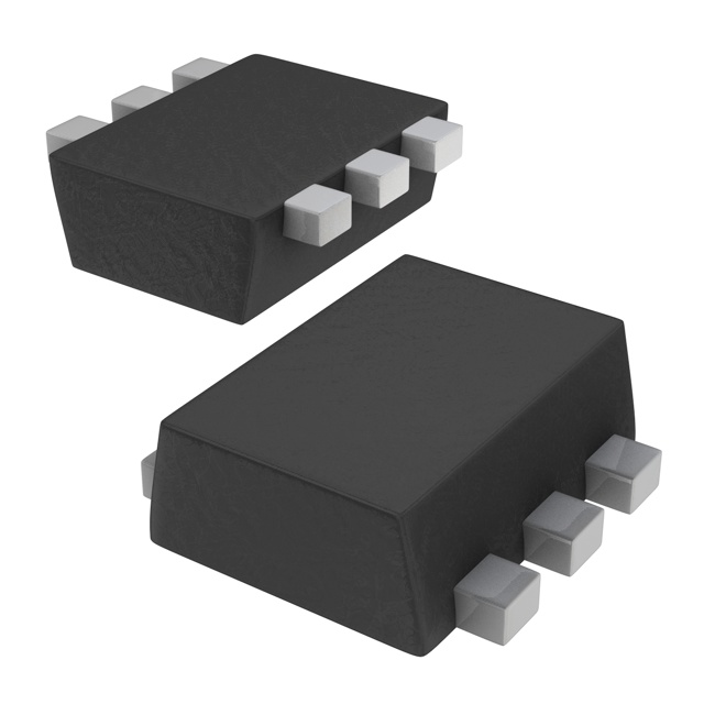
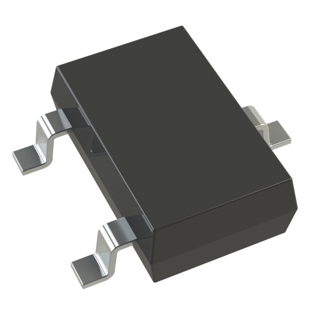
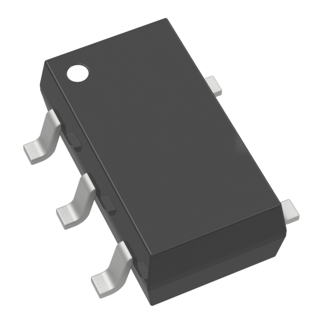
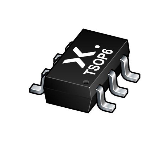
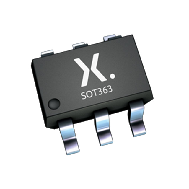
TRANS PREBIAS 1NPN 1PNP SOT666
- In stock 8,000

PEMD3 Datasheet Summary
Product Overview
The PEMD3 is a 50V, 100mA NPN/PNP resistor-equipped double transistor designed for low current applications. It features built-in bias resistors (R1 = 10kΩ, R2 = 10kΩ) and is housed in an ultra-small and flat lead SOT666 Surface-Mounted Device (SMD) plastic package. This device simplifies circuit design by reducing component count and pick-and-place costs.
Features
- Output Current Capability: 100mA
- Built-in Bias Resistors: R1 = 10kΩ, R2 = 10kΩ
- Simplifies Circuit Design: Reduces component count and assembly costs
- Suitable for Low Current Applications: Ideal for peripheral drivers and controlling IC inputs
Applications
- Low Current Peripheral Driver: Suitable for driving low current devices
- Controlling IC Inputs: Ideal for digital applications
- Replaces General-Purpose Transistors: Can be used in various digital applications
Quick Reference Data
TableCopy
| Parameter | Conditions | Min | Typ | Max | Unit |
|---|---|---|---|---|---|
| Collector-Emitter Voltage (VCEO) | Open base | - | 1 | 50 | V |
| Output Current (IO) | - | - | - | 100 | mA |
| Bias Resistor 1 (R1) | [1] | 7 | 10 | 13 | kΩ |
| Bias Resistor Ratio (R2/R1) | [1] | 0.8 | 1 | 1.2 | - [1] See "Section 11: Test Information" for resistor calculation and test conditions. |
Pinning Information
TableCopy
| Pin | Symbol | Description |
|---|---|---|
| 1 | GND1 | Ground (emitter) TR1 |
| 2 | 1 | Input (base) TR1 |
| 3 | 02 | Output (collector) TR2 |
| 4 | 12 | Input (base) TR2 |
| 5 | 01 | Output (collector) TR1 |
Ordering Information
- Type Number: PEMD3
- Package: SOT666 (plastic, surface-mounted package; 6 leads; 0.5 mm pitch; 1.6mm x 1.2mm x 0.55mm body)
- Version: SOT666
Marking
- Marking Code: D3
Limiting Values
TableCopy
| Parameter | Conditions | Min | Max | Unit |
|---|---|---|---|---|
| Collector-Base Voltage (VCBO) | Open emitter | - | 50 | V |
| Collector-Emitter Voltage (VCEO) | Open base | - | 50 | V |
| Emitter-Base Voltage (VEBO) | Open collector | -40 | -10 | V |
| Input Voltage (VI) | - | -10 | -40 | V |
| Output Current (IO) | - | - | 100 | mA |
| Total Power Dissipation (Ptot) | Tamb ≤ 25°C | - | 200 | mW (per transistor) |
| Total Power Dissipation (Ptot) | Tamb ≤ 25°C | - | 300 | mW (per device) |
| Junction Temperature (Tj) | - | - | 150 | °C |
| Ambient Temperature (Tamb) | -65 | 150 | °C | |
| Storage Temperature (Tstg) | -65 | 150 | °C |
Thermal Characteristics
TableCopy
| Parameter | Conditions | Min | Typ | Max | Unit |
|---|---|---|---|---|---|
| Junction to Ambient Thermal Resistance (Rth(j-a)) | [1] | - | 625 | K/W (per transistor) | |
| Junction to Ambient Thermal Resistance (Rth(j-a)) | [1] | - | 417 | K/W (per device) [1] Device mounted on an FR4 Printed-Circuit Board (PCB), single-sided, 35μm copper, tin-plated, and standard footprint. |
Characteristics
TableCopy
| Parameter | Conditions | Min | Typ | Max | Unit |
|---|---|---|---|---|---|
| Collector-Base Breakdown Voltage (V(BR)CBO) | IC = 100 µA, IE = 0 A, Tamb = 25°C | 50 | - | - | V |
| Collector-Emitter Breakdown Voltage (V(BR)CEO) | IC = 2 mA, IB = 0 A, Tamb = 25°C | 50 | - | - | V |
| Collector-Base Cut-Off Current (ICBO) | VCB = 50 V, IE = 0 A, Tamb = 25°C | - | - | 100 | nA |
| Collector-Emitter Cut-Off Current (ICEO) | VCE = 30 V, IB = 0 A, Tamb = 25°C | - | - | 1 | µA |
| Emitter-Base Cut-Off Current (IEBO) | VEB = 5 V, IC = 0 mA, Tamb = 25°C | - | - | 400 | µA |
| DC Current Gain (hFE) | VCE = 5 V, IC = 5 mA, Tamb = 25°C | 30 | - | - | - |
| Collector-Emitter Saturation Voltage (VCEsat) | IC = 10 mA, IB = 0.5 mA, Tamb = 25°C | - | - | 150 | mV |
| Off-State Input Voltage (VI(off)) | VCE = 5 V, IC = 100 µA, Tamb = 25°C | - | 1.1 | 0.8 | V |
| On-State Input Voltage (VI(on)) | VCE = 0.3 V, IC = 10 mA, Tamb = 25°C | 2.5 | 1.8 | - | V |
| Bias Resistor 1 (R1) | [1] | 7 | 10 | 13 | kΩ |
| Bias Resistor Ratio (R2/R1) | [1] | 0.8 | 1 | 1.2 | - [1] See "Section 11: Test Information" for resistor calculation and test conditions. |
Package Outline
- Package Type: SOT666
- Dimensions: 1.6mm x 1.2mm x 0.55mm body, 0.5 mm pitch, 6 leads
Soldering Information
- Reflow Soldering Footprint: Suitable for SOT666 package
- Solder Lands: 0.4mm (6x)
- Placement Area: 1.075mm x 0.55mm
- Solder Paste Occupied Area: 0.325mm x 0.375mm (4x)
Revision History
- Document ID: PEMD3v.12
- Release Date: 2022-12-28
- Changes: Family data sheet reduced to single type data sheet. Product(s) changed to non-automotive qualification.
Purchase
No need to register to order from JMChip Electronics, but signing in lets you track your order like a pro. Give it a try for a smoother shopping ride.
Means
Easy peasy! Pay your way with PayPal, Credit Card, or wire transfer in USD. We've got you covered.
RFQ(Request for Quotations)
Get the freshest prices and stock updates by asking for a quote! Our sales team will shoot you an email within a day. It's that simple.
IMPORTANT NOTICE
1. Look out for your order details in your inbox! (If it's missing, check the spam folder just in case.)
2. Our sales manager will double-check the order and keep you posted on any price or stock changes. No worries, we've got you covered.

Shipping Rate
We ship orders once a day around 5 p.m., except Sunday. Once shipped, the estimated delivery time depends on the courier company you choose, usually 5-7 working days.

Shipping Methods
We provide DHL, FedEx, UPS, EMS, SF Express, and Registered Air Mail international shipping.


Payment
You can pay the orders on the website directly or pay by wire transfer offline. We support: Paypal、VISA、Credit Card.


Nexperia USA Inc.
Nexperia USA Inc.
Nexperia USA Inc.
Nexperia USA Inc.
Nexperia USA Inc.
Nexperia USA Inc.
Nexperia USA Inc.
Nexperia USA Inc.
Nexperia USA Inc.
Nexperia USA Inc.
Nexperia USA Inc.
Nexperia USA Inc.