
Nexperia USA Inc. 74AUP2G98GUX


- Part Number:
74AUP2G98GUX
- Manufacturer:
- Category:
- RoHs:
 RoHS Compliant
 - Datasheet:
 74AUP2G98GUX_Datesheet
 - Description:
IC PROG GATE W/SCHMITT 10XQFN
- In stock 0

74AUP2G98GU Model Information
Overview
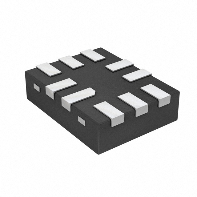
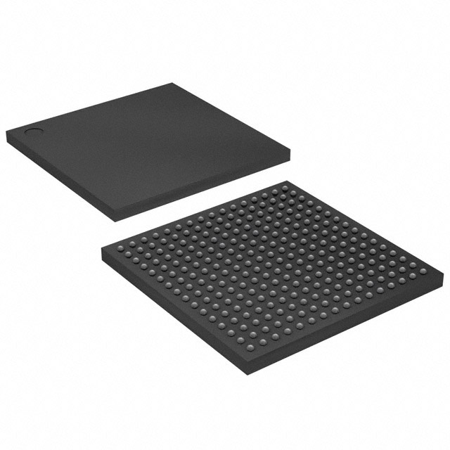
The 74AUP2G98GU is a low-power dual PCB configurable multiple function gate from Nexperia. It is designed for applications requiring efficient signal processing with minimal power consumption. This model is housed in an XQFN10 package, which is a plastic, extremely thin quad flat package with no leads and a body size of 1.40 × 1.80 × 0.50 mm.
Ordering Information
- Type Number: 74AUP2G98GU
- Temperature Range: -40°C to +125°C
- Package: XQFN10
- Description: Plastic, extremely thin quad flat package; no leads; 10 terminals; body 1.40 × 1.80 × 0.50 mm
- Version: SOT1160-1
Marking
- Marking Code: a9
- Pin 1 Indicator: Located on the lower left corner of the device, below the marking
Functional Diagram
The functional diagram of the 74AUP2G98GU includes logic symbols and IEC logic symbols, illustrating the dual gate functions.
Pinning Information
Pin Configuration
- 1A: Pin 10
- 1B: Pin 1
- 1C: Pin 2
- 1Y: Pin 8
- 2A: Pin 5
- 2B: Pin 6
- 2C: Pin 7
- 2Y: Pin 3
- GND: Pin 4
- VCC: Pin 9
Pin Description
- 1A, 2A: Data input
- 1B, 2B: Data input
- 1C, 2C: Data input
- 1Y, 2Y: Data output
- GND: Ground (0 V)
- VCC: Supply voltage
Functional Description
The 74AUP2G98GU provides the following functions:
- 2-input MUX with inverted output
- 2-input NAND
- 2-input NOR with one input inverted
- 2-input AND with one input inverted
- 2-input NAND with one input inverted
- 2-input OR with one input inverted
- 2-input NOR
- Buffer
- Inverter
Limiting Values
- Supply Voltage (VCC): -0.5 V to +4.6 V
- Input Clamping Current (IIK): -50 mA (for VI < 0 V)
- Input Voltage (VI): -0.5 V to +4.6 V
- Output Clamping Current (IOK): -50 mA (for VO < 0 V)
- Output Voltage (VO): -0.5 V to +4.6 V (Active mode and Power-down mode)
- Output Current (IO): ±20 mA (for VO = 0 V to VCC)
- Supply Current (ICC): 50 mA
- Ground Current (IGND): -50 mA
- Storage Temperature (Tstg): -65°C to +150°C
- Total Power Dissipation (Ptot): 250 mW (at Tamb = -40°C to +125°C)
Recommended Operating Conditions
- Supply Voltage (VCC): 0.8 V to 3.6 V
- Input Voltage (VI): 0 V to 3.6 V
- Output Voltage (VO): 0 V to VCC (Active mode); 0 V to 3.6 V (Power-down mode)
- Ambient Temperature (Tamb): -40°C to +125°C
Static Characteristics
- High-Level Output Voltage (VOH): Varies with VCC and output current (VCC - 0.1 V to 2.72 V)
- Low-Level Output Voltage (VOL): Varies with VCC and output current (0.1 V to 0.44 V)
- Input Leakage Current (II): ±0.1 μA
- Power-Off Leakage Current (IOFF): ±0.2 μA
- Additional Power-Off Leakage Current (ΔIOFF): 0.5 μA
- Supply Current (ICC): 40 μA
- Additional Supply Current (ΔICC): 40 μA
- Input Capacitance (CI): 1.1 pF
- Output Capacitance (CO): 1.7 pF
Dynamic Characteristics
- Propagation Delay (tpd): Varies with VCC and load capacitance (CL)For CL = 5 pF: 1.9 ns to 23.3 nsFor CL = 10 pF: 2.3 ns to 27.1 nsFor CL = 15 pF: 2.5 ns to 30.6 nsFor CL = 30 pF: 2.9 ns to 38.7 ns
Package Outline
- Package Type: XQFN10 (SOT1160-1)
- Dimensions:A: 0.5 mmA1: 0.05 mmA2: 0.25 mmb: 1.5 mmD: 1.9 mmE: 0.45 mme: 0.55 mmL: 0.4 mmL1: 0.40 mmV: 0.50 mmW: 0.1 mmy: 0.05 mmy1: 0.05 mm
Abbreviations
- CDM: Charged Device Model
- DUT: Device Under Test
- ESD: ElectroStatic Discharge
- HBM: Human Body Model
- PCB: Printed-Circuit Board
Purchase
No need to register to order from JMChip Electronics, but signing in lets you track your order like a pro. Give it a try for a smoother shopping ride.
Means
Easy peasy! Pay your way with PayPal, Credit Card, or wire transfer in USD. We've got you covered.
RFQ(Request for Quotations)
Get the freshest prices and stock updates by asking for a quote! Our sales team will shoot you an email within a day. It's that simple.
IMPORTANT NOTICE
1. Look out for your order details in your inbox! (If it's missing, check the spam folder just in case.)
2. Our sales manager will double-check the order and keep you posted on any price or stock changes. No worries, we've got you covered.

Shipping Rate
We ship orders once a day around 5 p.m., except Sunday. Once shipped, the estimated delivery time depends on the courier company you choose, usually 5-7 working days.

Shipping Methods
We provide DHL, FedEx, UPS, EMS, SF Express, and Registered Air Mail international shipping.


Payment
You can pay the orders on the website directly or pay by wire transfer offline. We support: Paypal、VISA、Credit Card.


Nexperia USA Inc.
Nexperia USA Inc.
Nexperia USA Inc.
Nexperia USA Inc.
Nexperia USA Inc.
Nexperia USA Inc.
Nexperia USA Inc.
Nexperia USA Inc.
Nexperia USA Inc.
Nexperia USA Inc.
Nexperia USA Inc.
Nexperia USA Inc.