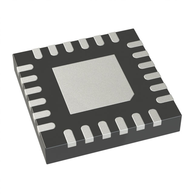
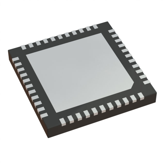
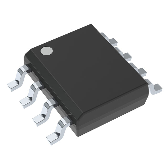
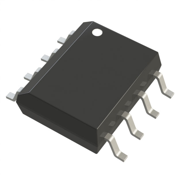
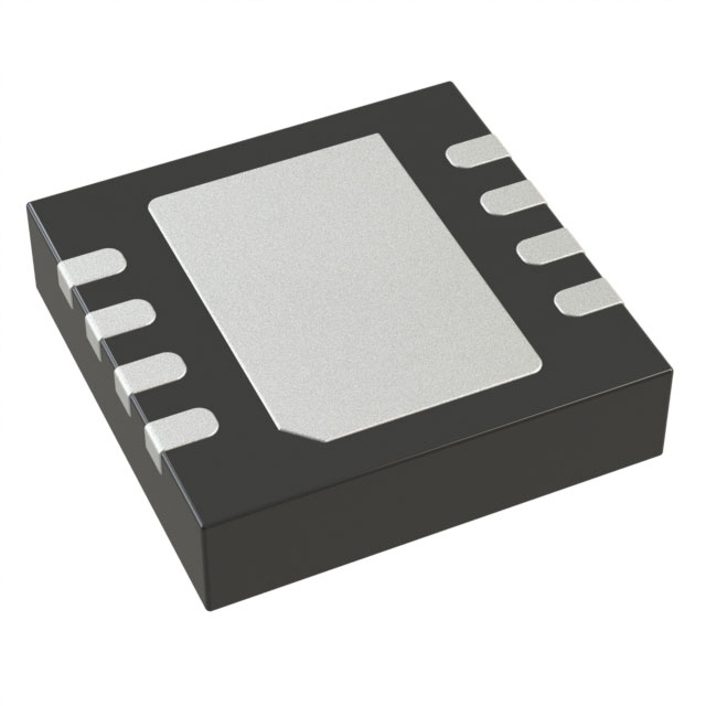
Nexperia USA Inc. 74HC5555D,112


- Part Number:
74HC5555D,112
- Manufacturer:
- Category:
- RoHs:
 RoHS Compliant
 - Datasheet:
 74HC5555D,112_Datesheet
 - Description:
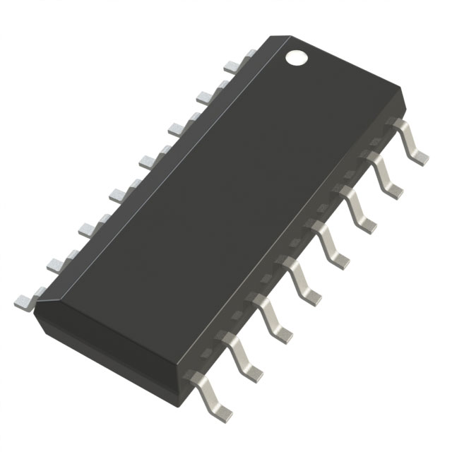
IC OSC TIMER W/OSC 89MHZ 16SOIC
- In stock 0
Model Information for 74HC5555D,112
General Description
The 74HC5555D,112 is a precision programmable delay timer with an oscillator. It features a 24-stage binary counter, integrated oscillator (using external timing components), retriggerable/non-retriggerable monostable, automatic power-ON reset, output control logic, oscillator control logic, and overriding asynchronous master reset.
Features and Benefits
- Supply Voltage Range: 2.0V to 6.0V
- CMOS Input Levels: Compatible with standard CMOS logic levels.
- Edge Triggering: Both positive and negative edge triggered.
- Retriggerable/Non-retriggerable: Flexible triggering options.
- Programmable Delay:Minimum: 100nsMaximum: Depends on input frequency and division ratio.
- Divide-by Range: From 2 to 224.
- Direct Reset: Terminates output pulse immediately.
- Low Power Consumption: In triggered start mode.
- Oscillator Modes:RC oscillatorCrystal oscillatorExternal oscillator
- Unaffected by Variations: Temperature and VCC variations when using an external oscillator.
- Automatic Power-ON Reset: Ensures reliable operation.
- Schmitt Trigger Action: On both trigger inputs for noise immunity.
- Direct Drive: Capable of driving a power transistor.
- High Precision: Due to digital timing.
- Compliance: Meets JEDEC standard no.7A.
- ESD Protection:HBM: Exceeds 2000V (EIA/JESD22-A114A)MM: Exceeds 200V (EIA/JESD22-A115-A)
- Temperature Range: Specified from -40°C to +85°C and -40°C to +125°C.
Applications
- Motor control
- Delay circuits
- Precision timing
- Domestic appliances
Ordering Information
- Package Type: SOT109-1
- Type Number: 74HC5555D
- Temperature Range: -40°C to +125°C
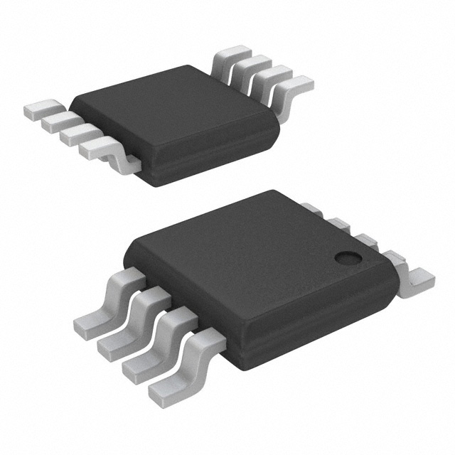
- Package Description: Plastic small outline package; 16 leads; body width 3.9 mm.
Functional Description
The 74HC5555D,112 incorporates an oscillator that can be configured in RC or crystal modes. It also supports external clock operation. The device features a 24-stage counter that can be digitally programmed via select inputs (S0 to S3) to achieve long pulse durations. The device can be triggered on either positive or negative edges and supports retriggering for extended pulse widths.
Pinning Information
Pin Configuration
- RS (Pin 1): Clock input/oscillator pin.
- RTC (Pin 2): External resistor connection.
- CTC (Pin 3): External capacitor connection.
- A (Pin 4): Positive-edge triggered trigger input.
- B (Pin 5): Negative-edge triggered trigger input.
- RTR/RTR (Pin 6): Retriggerable/non-retriggerable input.
- Q (Pin 7): Pulse output (active LOW).
- GND (Pin 8): Ground (0V).
- Q (Pin 9): Pulse output (active HIGH).
- S0, S1, S2, S3 (Pins 10, 11, 12, 13): Programmable input.
- OSC CON (Pin 14): Oscillator control.
- MR (Pin 15): Master reset input (active HIGH).
- VCC (Pin 16): Supply voltage.
Limiting Values
- Supply Voltage (VCC): -0.5V to +7V
- Input Clamping Current (IIK): ±20mA
- Output Clamping Current (IOK): ±20mA
- Output Current (IO): ±35mA
- Supply Current (ICC): 70mA
- Ground Current (IGND): -70mA to 0mA
- Storage Temperature (Tstg): -65°C to +150°C
- Total Power Dissipation (Ptot): 500mW (derates linearly with 8mW/K above 70°C for SO16 package)
Recommended Operating Conditions
- Supply Voltage (VCC): 2.0V to 6.0V
- Input Voltage (VI): 0V to VCC
- Output Voltage (VO): 0V to VCC
- Input Transition Rate (Δt/ΔV):VCC = 2.0V: 625ns/VVCC = 4.5V: 1.67 to 139ns/VVCC = 6.0V: 83ns/V
- Ambient Temperature (Tamb): -40°C to +125°C
Static Characteristics
Input Voltages
- VIH (HIGH-level input voltage):VCC = 2.0V: 1.5VVCC = 4.5V: 3.15VVCC = 6.0V: 4.2V
- VIL (LOW-level input voltage):VCC = 2.0V: 0.8VVCC = 4.5V: 2.1VVCC = 6.0V: 2.8V
Output Voltages
- VOH (HIGH-level output voltage):VCC = 2.0V; IO = -20μA: 1.9VVCC = 4.5V; IO = -20μA: 4.4VVCC = 6.0V; IO = -20μA: 5.9V
- VOL (LOW-level output voltage):VCC = 2.0V; IO = 20μA: 0.1VVCC = 4.5V; IO = 20μA: 0.1VVCC = 6.0V; IO = 20μA: 0.1V
Dynamic Characteristics
Propagation Delays
- tpd (A, B to Q, Q):VCC = 2.0V: 77ns to 360nsVCC = 4.5V: 28ns to 72nsVCC = 6.0V: 22ns to 61ns
- tpd (MR to Q, Q):VCC = 2.0V: 61ns to 280nsVCC = 4.5V: 22ns to 56nsVCC = 6.0V: 18ns to 48ns
- tpd (RS to Q, Q):VCC = 2.0V: 83ns to 375nsVCC = 4.5V: 30ns to 75nsVCC = 6.0V: 24ns to 64ns
Transition Times
- tt (Q, Q outputs):VCC = 2.0V: 19ns to 110nsVCC = 4.5V: 7ns to 22nsVCC = 6.0V: 6ns to 19ns
Application Information
Timing Component Limitations
- Oscillator Frequency: Determined by RtCt.
- Recommended Values:Ct: >50pF, up to any practical value.Rt: 10kΩ < Rt < 1MΩ.
- Avoid Start-up Problems: Rt >> 1kΩ.
Typical Crystal Oscillator
- Power Limiting Resistor (R2): 2.2kΩ recommended.
- Above 14MHz: Replace R2 with a capacitor (35pF typical).
Accuracy
- Device Accuracy: Better than 1% for short time delays (≥400ns).
- Tolerances: Dependent on external components.
Start-up Using External Clock
- Timing Pulse Initiation: Asynchronous to the oscillator clock.
- Clock HIGH/Low Effects:
- CopyShare
- Timing pulse may be lengthened or shortened by tW/2 (clock pulse width).
Start-up Using RC Oscillator
- First Clock Cycle: ≈35% longer than expected.
- Mitigation: Select more delay stages.
Start-up Using Crystal Oscillator
- Start-up Time: At least two clock cycles plus an unspecified period.
- Mode Recommendation: Continuous running mode (OSC CON = HIGH) to prevent delays.
Termination of the Timing Pulse
- Synchronization: End of timing pulse synchronized with the falling edge of the oscillator clock.
- Errors: May occur with high clock frequencies and large number of stages.
Synchronization Limits
- Clock Frequency Limits:1 Stage: 18MHz2 Stages: 14MHz3 Stages: 11MHz4 Stages: 9.6MHz24 Stages: 2.4MHz
Minimum Output Pulse Width
- Determination: Based on minimum clock pulse width plus maximum propagation delay.
- Accuracy: Minimum programmed pulse width of 100ns may be 4% to 10% too long.
Package Outline
- Package Type: SOT109-1 (SO16)
- Dimensions:Body Width: 3.9mmLead Count: 16 leads
Abbreviations
- CMOS: Complementary Metal-Oxide Semiconductor
- DUT: Device Under Test
- ESD: ElectroStatic Discharge
- HBM: Human Body Model
- MM: Machine Model
- TTL: Transistor-Transistor Logic
Revision History
- Document ID: 74HC5555 v.4
- Release Date: 2018-07-05
- Data Sheet Status: Product data sheet
- Change Notice: Redesigned to comply with Nexperia's identity guidelines. Legal texts adapted to the new company name. Type numbers 74HC5555N (SOT38-4), 74HCT5555N (SOT38-4), and 74HCT5555D (SOT109-1) removed.
Purchase
No need to register to order from JMChip Electronics, but signing in lets you track your order like a pro. Give it a try for a smoother shopping ride.
Means
Easy peasy! Pay your way with PayPal, Credit Card, or wire transfer in USD. We've got you covered.
RFQ(Request for Quotations)
Get the freshest prices and stock updates by asking for a quote! Our sales team will shoot you an email within a day. It's that simple.
IMPORTANT NOTICE
1. Look out for your order details in your inbox! (If it's missing, check the spam folder just in case.)
2. Our sales manager will double-check the order and keep you posted on any price or stock changes. No worries, we've got you covered.

Shipping Rate
We ship orders once a day around 5 p.m., except Sunday. Once shipped, the estimated delivery time depends on the courier company you choose, usually 5-7 working days.

Shipping Methods
We provide DHL, FedEx, UPS, EMS, SF Express, and Registered Air Mail international shipping.


Payment
You can pay the orders on the website directly or pay by wire transfer offline. We support: Paypal、VISA、Credit Card.


Nexperia USA Inc.
Nexperia USA Inc.

Nexperia USA Inc.

Nexperia USA Inc.

Nexperia USA Inc.

Nexperia USA Inc.

Nexperia USA Inc.
Nexperia USA Inc.
Nexperia USA Inc.
Nexperia USA Inc.

Nexperia USA Inc.

Nexperia USA Inc.


