
Allegro MicroSystems A4950ELJTR-T


- Part Number:
A4950ELJTR-T
- Manufacturer:
- Category:
- RoHs:
 Non-RoHS Compliant
 - Datasheet:
- Description:
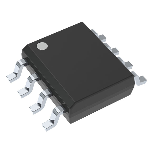
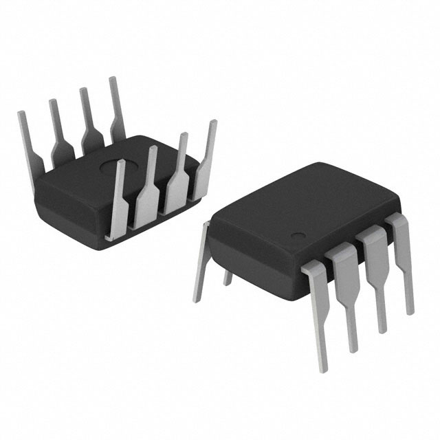
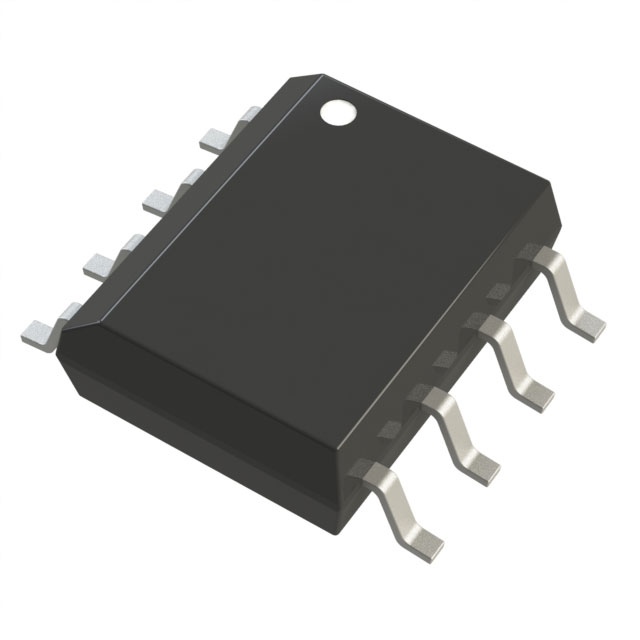
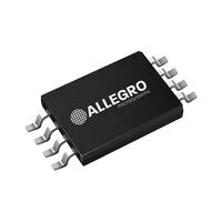
IC MOTOR DRIVER 8V-40V 8SOIC
- In stock 0

A4950ELJTR-T Full‑Bridge DMOS PWM Motor Driver – Complete Datasheet Summary
1. Basic Information
- Device Type: Full‑Bridge DMOS PWM Motor Driver
- Part Number: A4950ELJTR-T
- Grade: Commercial (E‑grade)
- Package: 8‑pin SOICN with exposed thermal pad (suffix LJ)
- Packing: 3000 pieces per 13‑inch reel
- Lead Status: Lead‑free (Pb‑free), 100% matte tin leadframe plating
- Qualification: Commercial grade (not AEC‑Q100)
- Target Applications: DC motor PWM speed & direction control
2. Key Features & Benefits
- Low on‑resistance RDS(on) DMOS outputs
- Adjustable PWM current limiting
- Internal synchronous rectification (lowers power dissipation)
- Overcurrent Protection (OCP):
- Low‑Power Standby mode
- Internal Undervoltage Lockout (UVLO)
- Crossover‑current (shoot‑through) protection
- Thermal shutdown with hysteresis
- Two‑wire logic control (IN1, IN2) for direction, speed, brake, coast
3. Operating Conditions
Temperature Ranges
- Ambient Operating Temperature (TA): −40 °C to +85 °C
- Maximum Junction Temperature (TJ max): 150 °C
- Storage Temperature: −55 °C to +150 °C
Voltage & Current
- Load Supply Voltage (VBB): 8 V to 40 V
- Continuous Output Current (IOUT): ±3.5 A (100% duty cycle)
- Transient Output Current (iOUT): ±6 A (tW < 500 ns)
- Logic Input Voltage (VIN): −0.3 V to +6 V
- VREF Input Voltage: 0 V to +5 V
- Sense Voltage (LSS pin): −0.5 V to +0.5 V
4. Absolute Maximum Ratings
表格
| Parameter | Symbol | Rating | Unit |
|---|---|---|---|
| Load Supply Voltage | VBB | 40 | V |
| Motor Output Voltage | VOUT | −2 to +42 | V |
| Logic Input Voltage | VIN | −0.3 to +6 | V |
| VREF Input Voltage | VREF | −0.3 to +6 | V |
| Sense Voltage (LSS) | VS | −0.5 to +0.5 | V |
| Continuous Output Current | IOUT | 3.5 | A |
| Transient Output Current | iOUT | 6 | A |
| Operating TA (E‑grade) | TA | −40 to +85 | °C |
| Max Junction Temp | TJ(max) | 150 | °C |
| Storage Temp | Tstg | −55 to +150 | °C |
5. Thermal Characteristics
表格
| Parameter | Condition | Value | Unit |
|---|---|---|---|
| Thermal Resistance RθJA | 2‑layer PCB (0.8 in² 2‑oz copper) | 62 | °C/W |
| Thermal Resistance RθJA | 4‑layer JEDEC standard PCB | 35 | °C/W |
6. Electrical Characteristics (TJ = 25 °C, VBB = 8–40 V)
General
表格
| Parameter | Symbol | Min | Typ | Max | Unit | |
|---|---|---|---|---|---|---|
| Total RDS(on) (source + sink) | – | – | 0.6 | 0.8 | Ω | @ IOUT = 2.5 A |
| Supply Current (IBB) | IBB | – | 10 | 20 | mA | fPWM < 30 kHz |
| Standby Supply Current | – | – | – | 10 | µA | Low‑Power mode |
| Body Diode Forward Voltage | Vf | – | – | 1.5 | V | @ If = ±2.5 A |
Logic Inputs
表格
| Parameter | Symbol | Min | Typ | Max | Unit |
|---|---|---|---|---|---|
| Logic High Voltage | VIN(1) | 2.0 | – | – | V |
| Logic Low Voltage | VIN(0) | – | – | 0.8 | V |
| Standby Threshold | VIN(STANDBY) | – | – | 0.4 | V |
| Input Hysteresis | VHYS | – | 250 | 550 | mV |
Timing
表格
| Parameter | Symbol | Min | Typ | Max | Unit |
|---|---|---|---|---|---|
| Crossover Delay | tCOD | 50 | – | 500 | ns |
| Blank Time | tBLANK | 2 | 3 | 4 | µs |
| Fixed Off‑Time | toff | 16 | 25 | 34 | µs |
| Standby Entry Delay | tst | – | 1 | 1.5 | ms |
| Power‑Up Delay | tpu | – | – | 30 | µs |
Protection Circuits
表格
| Parameter | Symbol | Min | Typ | Max | Unit |
|---|---|---|---|---|---|
| UVLO Threshold (rising VBB) | VBBUVLO | 7.0 | 7.5 | 7.95 | V |
| UVLO Hysteresis | VBBUVLOhys | – | 500 | – | mV |
| Thermal Shutdown Temp | TJTSD | – | 160 | – | °C |
| Thermal Shutdown Hysteresis | TSDhys | – | 15 | – | °C |
7. Pin Configuration (8‑Pin SOICN LJ)
表格
| Pin No. | Name | Function |
|---|---|---|
| 1 | GND | Ground |
| 2 | IN2 | Logic control input 2 |
| 3 | IN1 | Logic control input 1 |
| 4 | VREF | Current‑limit reference input |
| 5 | VBB | Motor power supply input |
| 6 | OUT1 | Full‑bridge output 1 |
| 7 | LSS | Current sense resistor connection |
| 8 | OUT2 | Full‑bridge output 2 |
| PAD | Exposed thermal pad | Enhanced heat dissipation |
8. PWM Control Truth Table
表格
| IN1 | IN2 | 10×VS > VREF | OUT1 | OUT2 | Function |
|---|---|---|---|---|---|
| 0 | 1 | False | L | H | Reverse |
| 1 | 0 | False | H | L | Forward |
| 0 | 1 | True | H/L | L | Chop (mixed decay), Reverse |
| 1 | 0 | True | L | H/L | Chop (mixed decay), Forward |
| 1 | 1 | False | L | L | Brake (slow decay) |
| 0 | 0 | False | Z | Z | Coast → Standby after 1 ms |
| Z = high‑impedance state |
9. Functional Description
Device Operation
- Full N‑channel DMOS bridge with synchronous rectification
- Fixed off‑time PWM current regulation
- IN1 / IN2 provide simple two‑wire control
Standby Mode
- Activated when IN1 and IN2 are low for >1 ms
- Reduces quiescent current to ~10 µA
- Wake‑up delay: max 30 µs
Current Limit Formula
Max trip current:
ITripMAX=10×RSVREF
- VREF = voltage at VREF pin (V)
- RS = external current‑sense resistor (Ω)
Protection Mechanisms
- Overcurrent Protection (OCP): latches outputs on short
- Thermal Shutdown: disables outputs at ~160 °C
- UVLO: blocks operation until VBB is valid
- Crossover‑current protection prevents shoot‑through
10. Application Information
Recommended External Components
- Current‑sense resistor RS: 0.25 Ω (for 2 A at VREF = 5 V)
- Decoupling capacitors:
PCB Layout Guidelines
- Solid, thick ground plane
- Exposed thermal pad soldered directly to PCB with thermal vias
- Star ground near LSS / GND
- Short, direct traces for power paths (OUT1, OUT2, VBB)
11. Typical Applications
- DC motor speed & direction control
- Robotics & small actuators
- Consumer electronics
- Industrial low‑voltage motion control
- Battery‑powered motor drives
Purchase
No need to register to order from JMChip Electronics, but signing in lets you track your order like a pro. Give it a try for a smoother shopping ride.
Means
Easy peasy! Pay your way with PayPal, Credit Card, or wire transfer in USD. We've got you covered.
RFQ(Request for Quotations)
Get the freshest prices and stock updates by asking for a quote! Our sales team will shoot you an email within a day. It's that simple.
IMPORTANT NOTICE
1. Look out for your order details in your inbox! (If it's missing, check the spam folder just in case.)
2. Our sales manager will double-check the order and keep you posted on any price or stock changes. No worries, we've got you covered.

Shipping Rate
We ship orders once a day around 5 p.m., except Sunday. Once shipped, the estimated delivery time depends on the courier company you choose, usually 5-7 working days.

Shipping Methods
We provide DHL, FedEx, UPS, EMS, SF Express, and Registered Air Mail international shipping.


Payment
You can pay the orders on the website directly or pay by wire transfer offline. We support: Paypal、VISA、Credit Card.


Allegro MicroSystems
Allegro MicroSystems
Allegro MicroSystems
Allegro MicroSystems
Allegro MicroSystems
Allegro MicroSystems