
Renesas CA3083M96


- Part Number:
CA3083M96
- Manufacturer:
- Category:
- RoHs:
 Non-RoHS Compliant
 - Datasheet:
 CA3083M96_Datesheet
 - Description:
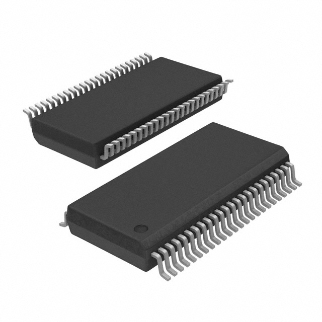
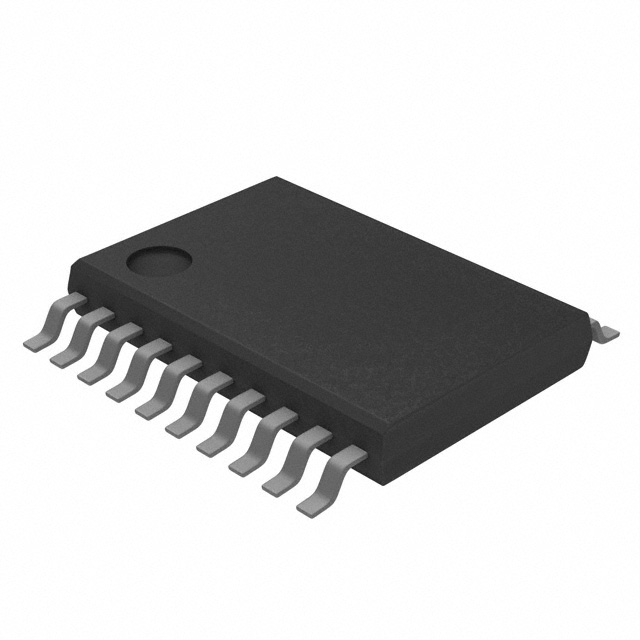
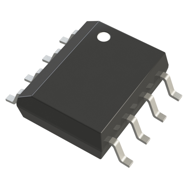
TRANS 5NPN 15V 0.1A 16SOIC
- In stock 0

Information of CA3083M96 NPN Transistor Array
Basic Overview
- Product Type: General-purpose high-current NPN transistor array
- Manufacturer: Intersil Corporation
- Document Reference: FN481.7 (December 15, 2011)
- Core Configuration: 5 independent high-current NPN transistors on a common monolithic substrate; Q1 and Q2 are matched for low-offset applications
- Key Features: High collector current (up to 100mA), low saturation voltage, separate substrate connection, Pb-free RoHS-compliant, wide operating temperature range
- Target Applications: Signal processing/switching (DC to VHF), lamp/relay drivers, differential amplifiers, temperature-compensated amplifiers, thyristor firing
Core Specifications
1. Absolute Maximum Ratings (Per Transistor)
| Parameter | Specification |
|---|---|
| Collector-to-Emitter Voltage (VCEO) | 15V |
| Collector-to-Base Voltage (VCBO) | 20V |
| Collector-to-Substrate Voltage (VCIO) | 20V |
| Emitter-to-Base Voltage (VEBO) | 5V (Min), 6.9V (Typ) |
| Collector Current (IC) | 100mA (Max) |
| Base Current (IB) | 20mA (Max) |
| Maximum Power Dissipation (Per Transistor) | 500mW |
| Junction Temperature (Plastic Package) | 150°C (Max) |
| Storage Temperature Range | -65°C to 150°C |
| Lead Temperature (Soldering, 10s) | 300°C (SOIC, lead tips only) |
2. Thermal Characteristics (SOIC Package)
| Parameter | Specification |
|---|---|
| Thermal Resistance (θJA) | 200°C/W (Typ) |
| Thermal Resistance (θJC) | N/A |
3. Electrical Performance (TA=25°C)
| Parameter | Symbol | Test Conditions | Min | Typ | Max | Units |
|---|---|---|---|---|---|---|
| Collector-to-Base Breakdown Voltage | V(BR)CBO | IC=100μA, IE=0 | 20 | 60 | - | V |
| Collector-to-Emitter Breakdown Voltage | V(BR)CEO | IC=1mA, IB=0 | 15 | 24 | - | V |
| Collector-to-Substrate Breakdown Voltage | V(BR)CIO | ICI=100μA, IB=0, IE=0 | 20 | 60 | - | V |
| Collector Cutoff Current (CEO) | ICEO | VCE=10V, IB=0 | - | - | 10 | μA |
| Collector Cutoff Current (CBO) | ICBO | VCB=10V, IE=0 | - | - | 1 | μA |
| DC Forward Current Transfer Ratio | hFE | VCE=3V, IC=10mA | 40 | 76 | - | - |
| VCE=3V, IC=50mA | 40 | 75 | - | - | ||
| Base-to-Emitter Voltage | VBE | VCE=3V, IC=10mA | 0.65 | 0.74 | 0.85 | V |
| Collector-to-Emitter Saturation Voltage | VCE(SAT) | IC=50mA, IB=5mA | - | 0.40 | 0.70 | V |
| Gain Bandwidth Product | fT | VCE=3V, IC=10mA | - | 450 | - | MHz |
4. Matched Pair (Q1 & Q2, Differential Amplifier Configuration)
| Parameter | Symbol | Test Conditions | Typ | Max | Units |
|---|---|---|---|---|---|
| Absolute Input Offset Voltage | VIOL | VCE=3V, IC=1mA | 1.2 | 5 | mV |
| Absolute Input Offset Current | IIOL | VCE=3V, IC=1mA | 0.7 | 2.5 | μA |
Package and Mechanical Details
1. Package Specifications
| Parameter | Specification |
|---|---|
| Package Type | 16-lead SOIC (Small Outline Integrated Circuit) |
| Package Drawing Number | M16.15 |
| Packaging Method | Tape and Reel |
| Part Marking | 3083 |
| Lead Finish | 100% matte tin (Pb-free, RoHS compliant) |
| Moisture Sensitivity Level (MSL) | Meets IPC/JEDEC J-STD-020 requirements for Pb-free reflow |
2. Key Package Notes
- Pb-free compatibility: Suitable for both SnPb and Pb-free soldering operations
- Substrate Connection: Terminal 5 (separate substrate pin) must be connected to a voltage more negative than any collector voltage (or DC/signal ground) for transistor isolation
- SOIC Package Restriction: Soldering limited to lead tips only (300°C for 10s max)
Ordering and Compliance
| Orderable Part Number | Part Marking | Temperature Range | Package | Compliance |
|---|---|---|---|---|
| CA3083M96 | 3083 | -55°C to 125°C | 16-lead SOIC (Tape and Reel) | RoHS compliant, Pb-free |
Complementary Part Variants
- CA3083: 16-lead PDIP (through-hole, -55°C to 125°C)
- CA3083Z: 16-lead Pb-free PDIP (wave solder only)
- CA3083MZ: 16-lead Pb-free SOIC
- CA3083MZ96: 16-lead Pb-free SOIC (Tape and Reel)
Operational Guidelines
- Substrate Handling: Connect substrate terminal to ground (DC or AC) with a bypass capacitor to avoid cross-coupling between transistors
- Matching Usage: Utilize Q1 and Q2 for low-offset applications (e.g., differential amplifiers) to leverage their matched VBE and input offset parameters
- Temperature Considerations: Operate within -55°C to 125°C ambient temperature; hFE and VBE vary with temperature (refer to Typical Performance Curves)
- ESD Sensitivity: Follow proper IC handling procedures to prevent electrostatic discharge damage
Purchase
No need to register to order from JMChip Electronics, but signing in lets you track your order like a pro. Give it a try for a smoother shopping ride.
Means
Easy peasy! Pay your way with PayPal, Credit Card, or wire transfer in USD. We've got you covered.
RFQ(Request for Quotations)
Get the freshest prices and stock updates by asking for a quote! Our sales team will shoot you an email within a day. It's that simple.
IMPORTANT NOTICE
1. Look out for your order details in your inbox! (If it's missing, check the spam folder just in case.)
2. Our sales manager will double-check the order and keep you posted on any price or stock changes. No worries, we've got you covered.

Shipping Rate
We ship orders once a day around 5 p.m., except Sunday. Once shipped, the estimated delivery time depends on the courier company you choose, usually 5-7 working days.

Shipping Methods
We provide DHL, FedEx, UPS, EMS, SF Express, and Registered Air Mail international shipping.


Payment
You can pay the orders on the website directly or pay by wire transfer offline. We support: Paypal、VISA、Credit Card.


Renesas
Renesas
Renesas
Renesas
Renesas

Renesas
Renesas

Renesas
Renesas
Renesas
Renesas
Renesas