
Texas Instruments(TI) LMG5200MOFT


- Part Number:
LMG5200MOFT
- Manufacturer:
- Category:
- RoHs:
 RoHS Compliant
 - Datasheet:
 LMG5200MOFT_Datesheet
 - Description:
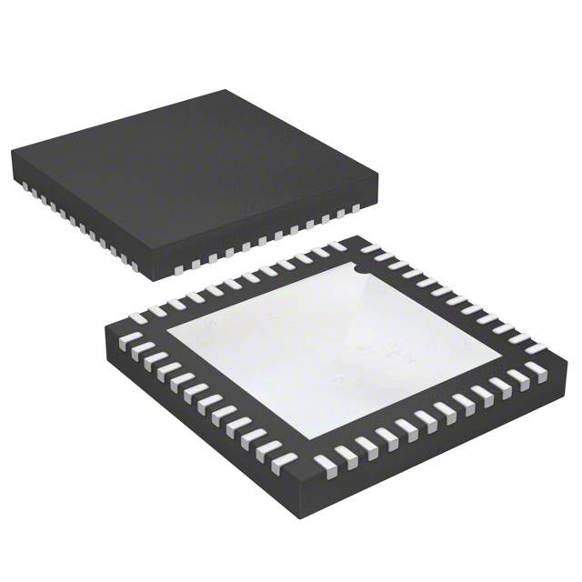
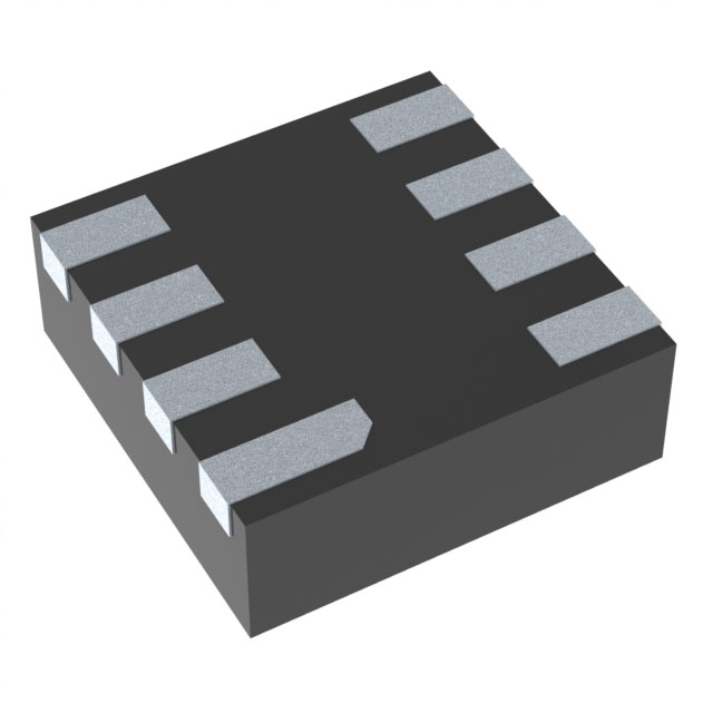
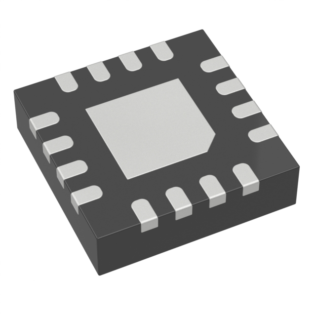
IC HALF BRIDGE DRIVER 10A 9QFN
- In stock 1,092

LMG5200MOF Model Information
Model Overview
- Model Number: LMG5200MOF
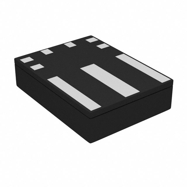
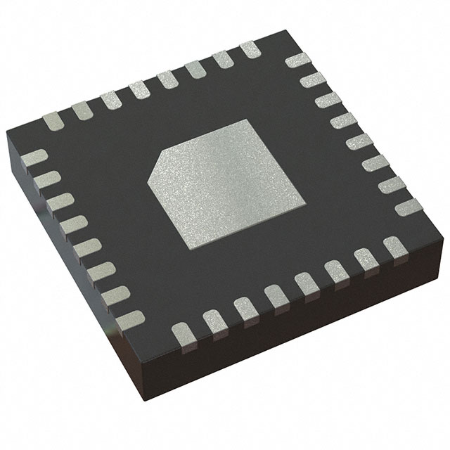
- Package Type: QFM (9-Pin)
- Operating Temperature Range: -40°C to +125°C
- Storage Temperature Range: -40°C to +150°C
- Features
- Integrated GaN FETs and Driver: 15-mΩ GaN FETs with high-frequency driver
- Voltage Rating: 80-V continuous, 100-V pulsed
- Package Optimization: Designed for easy PCB layout, eliminating the need for underfill, creepage, and clearance requirements
- Low Common Source Inductance: Ensures high slew rate switching without excessive ringing
- Ideal for Isolated and Non-Isolated Applications: Suitable for a wide range of applications
- Gate Driver Capability: Up to 10 MHz switching
- Internal Bootstrap Supply Voltage Clamping: Prevents GaN FET overdrive
- Supply Rail Undervoltage Lockout Protection: Ensures safe operation
- Excellent Propagation Delay and Matching: 29.5 ns typical, 2 ns typical mismatch
- Low Power Consumption
- Applications
- Wide VIN Multi-MHz Synchronous Buck Converters: High-frequency power conversion
- Class D Amplifiers for Audio: High-efficiency audio amplification
- 48-V Point-of-Load (POL) Converters: For telecom, industrial, and enterprise computing
- High Power Density Single- and Three-Phase Motor Drive: Efficient motor control
- Pin Configuration
- PIN 1: VIN (Input Voltage)
- PIN 2: HB (High-side gate driver bootstrap rail)
- PIN 3: HS (High-side GaN FET source connection)
- PIN 4: HI (High-side gate driver control input)
- PIN 5: LI (Low-side driver control input)
- PIN 6: VCC (5-V positive gate drive supply)
- PIN 7: AGND (Analog ground)
- PIN 8: SW (Switching node)
- PIN 9: PGND (Power ground)
- Specifications
- Absolute Maximum Ratings:VIN to PGND: 0 to 80 VVIN to PGND (pulsed, 100-ms max duration): 100 VHB to AGND: -0.3 to 86 VHS to AGND: -5 to 80 VHI to AGND: -0.3 to 12 VLI to AGND: -0.3 to 12 VVCC to AGND: -0.3 to 6 VHB to HS: -0.3 to 6 VHB to VCC: 0 to 80 VSW to PGND: -5 to 80 VIOUT from SW pin: 10 AJunction Temperature (TJ): -40 to 125 °CStorage Temperature (Tstg): -40 to 150 °C
- ESD Ratings:Human-body model (HBM): ±1000 VCharged-device model (CDM): ±500 V
- Recommended Operating Conditions:VCC: 4.75 V to 5.25 VLI or HI Input: 0 to 12 VVIN: 0 to 80 VHS, SW: -5 to 80 VHB: VHS+ 4 V to VHS+ 5.25 VHS, SW Slew rate: 50 V/nsJunction Temperature (TJ): -40 to 125 °C
- Thermal Information:Junction-to-ambient thermal resistance (RθJA): 35 °C/WJunction-to-case (top) thermal resistance (RθJC(top)): 18 °C/WJunction-to-board thermal resistance (RθJB): 16 °C/WJunction-to-top characterization parameter (ψJT): 1.8 °C/WJunction-to-board characterization parameter (ψJB): 16 °C/W
- Electrical Characteristics:ICC (VCC Quiescent Current): 0.08 mA to 0.125 mAICCO (Total VCC Operating Current): 3.0 mA to 5.0 mAIHB (HB Quiescent Current): 0.09 mA to 0.150 mAIHBO (HB Operating Current): 1.5 mA to 2.5 mAVIH (High-Level Input Voltage Threshold): 1.87 V to 2.22 VVIL (Low-Level Input Voltage Threshold): 1.48 V to 1.76 VVHYS (Hysteresis between rising and falling threshold): 400 mVR (Input pull-down resistance): 100 kΩ to 300 kΩVCCR (VCC Rising edge threshold): 3.2 V to 4.5 VVCC(hyst) (VCC UVLO threshold hysteresis): 200 mVVHBR (HB Rising edge threshold): 2.5 V to 3.9 VVHB(hyst) (HB UVLO threshold hysteresis): 200 mVVDL (Low-Current forward voltage): 0.45 V to 0.65 VVDH (High current forward voltage): 0.9 V to 1.0 VRD (Dynamic Resistance): 1.85 Ω to 2.8 ΩHB-HS Clamp Regulation Voltage: 4.65 V to 5.2 VtBS (Bootstrap diode reverse recovery time): 40 nsQRR (Bootstrap diode reverse recovery charge): 2 nCRDS(ON)HS (High-side GaN FET on-resistance): 15 mΩ to 20 mΩRDS(ON)LS (Low-side GaN FET on-resistance): 15 mΩ to 20 mΩVSD (GaN 3rd quadrant conduction drop): 2 VIL-VIN-SW (Leakage from VIN to SW): 25 µA to 150 µAIL-SW-GND (Leakage from SW to GND): 25 µA to 150 µACOSS (Output Capacitance of high-side GaN FET and low-side GaN FET): 266 pFQG (Total Gate Charge): 3.8 nCQOSS (Output Charge): 21 nCQRR (Source to Drain Reverse Recovery Charge): 0 nCtHIPLH (Propagation delay: HI Rising): 29.5 ns to 50 nstHIPHL (Propagation delay: HI Falling): 29.5 ns to 50 nstLPLH (Propagation delay: LI Rising): 29.5 ns to 50 nstLPHL (Propagation delay: LI Falling): 29.5 ns to 50 nstMON (Delay Matching: LI high & HI low): 2 ns to 8.0 nstMOFF (Delay Matching: LI low & HI high): 2 ns to 8.0 nstPW (Minimum Input Pulse Width that Changes the Output): 10 ns
- Ordering Information
- Part Number: LMG5200MOFR
- Description: QFM package, 9 pins, RoHS & Green, MSL3, 2000 pieces per reel
- Part Number: LMG5200MOFT
- Description: QFM package, 9 pins, RoHS & Green, MSL3, 250 pieces per reel
- Mechanical Information
- Package Outline: QFM - 2 mm max height MOF0009A
- Dimensions: 6.00 mm × 8.00 mm × 2.00 mm
- Layout Guidelines
- Power Loop Optimization: Minimize power loop impedance by placing return path directly underneath the first layer.
- Capacitor Placement: Place VCC and bootstrap capacitors as close as possible to the device.
- AGND Connection: Do not directly connect AGND to PGND to avoid noise injection.
- SW Node Capacitance: Minimize capacitance by using minimal copper
Purchase
No need to register to order from JMChip Electronics, but signing in lets you track your order like a pro. Give it a try for a smoother shopping ride.
Means
Easy peasy! Pay your way with PayPal, Credit Card, or wire transfer in USD. We've got you covered.
RFQ(Request for Quotations)
Get the freshest prices and stock updates by asking for a quote! Our sales team will shoot you an email within a day. It's that simple.
IMPORTANT NOTICE
1. Look out for your order details in your inbox! (If it's missing, check the spam folder just in case.)
2. Our sales manager will double-check the order and keep you posted on any price or stock changes. No worries, we've got you covered.

Shipping Rate
We ship orders once a day around 5 p.m., except Sunday. Once shipped, the estimated delivery time depends on the courier company you choose, usually 5-7 working days.

Shipping Methods
We provide DHL, FedEx, UPS, EMS, SF Express, and Registered Air Mail international shipping.


Payment
You can pay the orders on the website directly or pay by wire transfer offline. We support: Paypal、VISA、Credit Card.


Texas Instruments(TI)
Texas Instruments(TI)
Texas Instruments(TI)
Texas Instruments(TI)
Texas Instruments(TI)
Texas Instruments(TI)
Texas Instruments(TI)
Texas Instruments(TI)
Texas Instruments(TI)
Texas Instruments(TI)
Texas Instruments(TI)
Texas Instruments(TI)