
Lattice Semiconductor Corporation LX64EC-5FN100C


- Part Number:
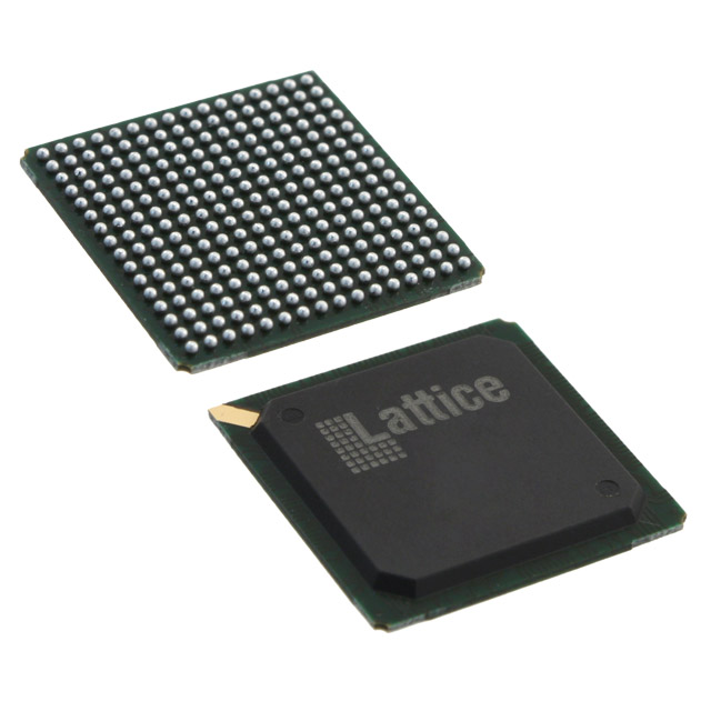
LX64EC-5FN100C
- Manufacturer:
- Category:
- RoHs:
 RoHS Compliant
 - Datasheet:
- Description:
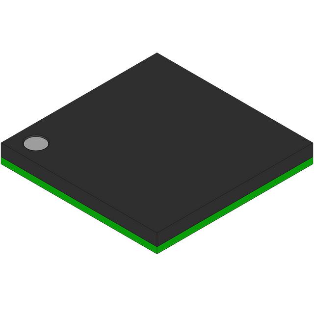
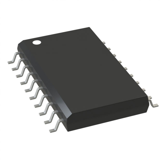
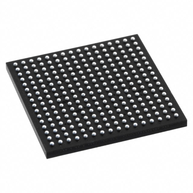
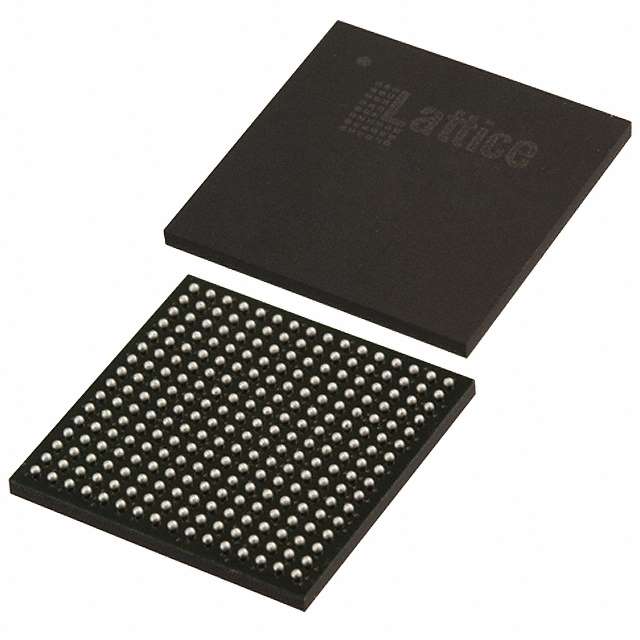
CROSSBAR SWITCH, CMOS, PBGA100
- In stock 1,168

LX64EC-5FN100C Device Information
Device Overview
- Device Family: ispGDX2™ Family
- Part Number: LX64EC-5FN100C
- Product Line: LX64EC (64 I/Os, 1.8V Core Voltage)
- Status: Discontinued (PCN#09-10)
Key Specifications
I/O Configuration
- Number of I/Os: 64
- I/O Banks: 8 banks (8 I/Os per bank)
- I/O Standards Supported:LVCMOS 1.8V, 2.5V, 3.3VLVTTLPCI 3.3, PCI-XSSTL 2/3 Class I & IIHSTL Class I, III, IVGTL+LVDS, Bus LVDSLVPECL
Performance Characteristics
- Propagation Delay (tPD): 5.0 ns
- Maximum Toggle Frequency: 180 MHz (without PLL)
- Maximum Clock Frequency with PLL: 180 MHz
- Maximum Bandwidth: 12.8 Gbps (with SERDES)
Power Requirements
- Core Voltage (VCC): 1.8V
- I/O Voltage (VCCO): 1.8V, 2.5V, or 3.3V (bank independent)
- PLL/HSI Voltage (VCCP): 1.8V
- JTAG Voltage (VCCJ): 1.8V
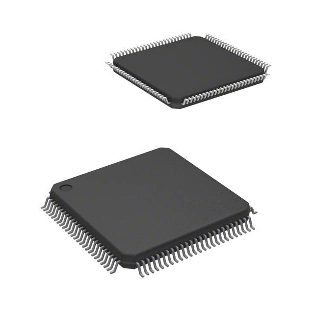
Package Information
- Package Type: Lead-Free 100-ball fpBGA
- Pin Count: 100
- Package Code: FN100C
- Temperature Grade: Commercial (0°C to 90°C junction temperature)
Features
High-Speed Serial Interface (sysHSI)
- SERDES Channels: Up to 4 channels (2 transmitters, 2 receivers)
- Data Rates: Up to 800 Mbps per channel
- Encoding Support: 8B/10B and 10B/12B
- Clock Data Recovery (CDR): Built-in
- Source Synchronous Support: Yes
Clock Management
- PLLs: 2 PLLs with frequency synthesis and skew management
- Global Clock Networks: 4 global clock nets
- Clock Shifting: Up to ±2.35ns in 335ps steps
Memory and Logic
- FIFOs: 4 FIFOs (10x15 words each)
- GDX Blocks: 4 blocks
- MRBs: 64 Multiplexer Register Blocks
- Maximum MUX Size: 188:1
Programming and Testing
- In-System Programming (ISP): IEEE 1532 compliant
- Boundary Scan: IEEE 1149.1 compliant
- Security: Programmable security bit prevents readback
- Hot Socketing: Supported
Ordering Information
- Commercial Grade: LX64EC-5FN100C
- Industrial Grade: LX64EC-5FN100I (available as separate part number)
Applications
- Multi-port multi-processor interfaces
- Wide data and address bus multiplexing
- Programmable control signal routing
- Programmable bus interfaces
- High-speed serial communications
Documentation References
- Data Sheet: ispGDX2 Family Data Sheet (September 2005)
- Technical Notes:TN1000: sysIO Design and Usage GuidelinesTN1020: sysHSI Usage GuidelinesTN1021: Power Estimation in ispGDX2 Devices
Purchase
No need to register to order from JMChip Electronics, but signing in lets you track your order like a pro. Give it a try for a smoother shopping ride.
Means
Easy peasy! Pay your way with PayPal, Credit Card, or wire transfer in USD. We've got you covered.
RFQ(Request for Quotations)
Get the freshest prices and stock updates by asking for a quote! Our sales team will shoot you an email within a day. It's that simple.
IMPORTANT NOTICE
1. Look out for your order details in your inbox! (If it's missing, check the spam folder just in case.)
2. Our sales manager will double-check the order and keep you posted on any price or stock changes. No worries, we've got you covered.

Shipping Rate
We ship orders once a day around 5 p.m., except Sunday. Once shipped, the estimated delivery time depends on the courier company you choose, usually 5-7 working days.

Shipping Methods
We provide DHL, FedEx, UPS, EMS, SF Express, and Registered Air Mail international shipping.


Payment
You can pay the orders on the website directly or pay by wire transfer offline. We support: Paypal、VISA、Credit Card.


Lattice Semiconductor Corporation
Lattice Semiconductor Corporation
Lattice Semiconductor Corporation
Lattice Semiconductor Corporation

Lattice Semiconductor Corporation