
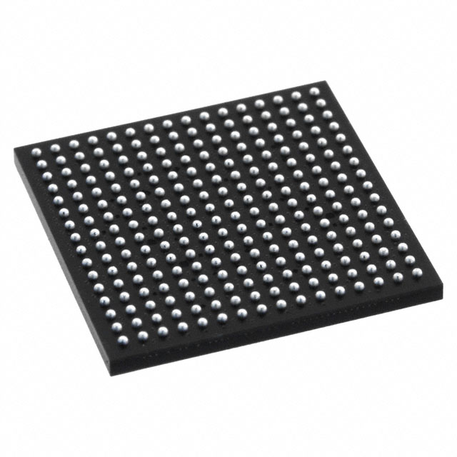
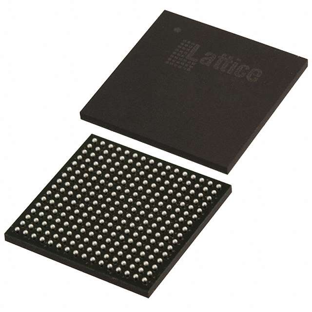
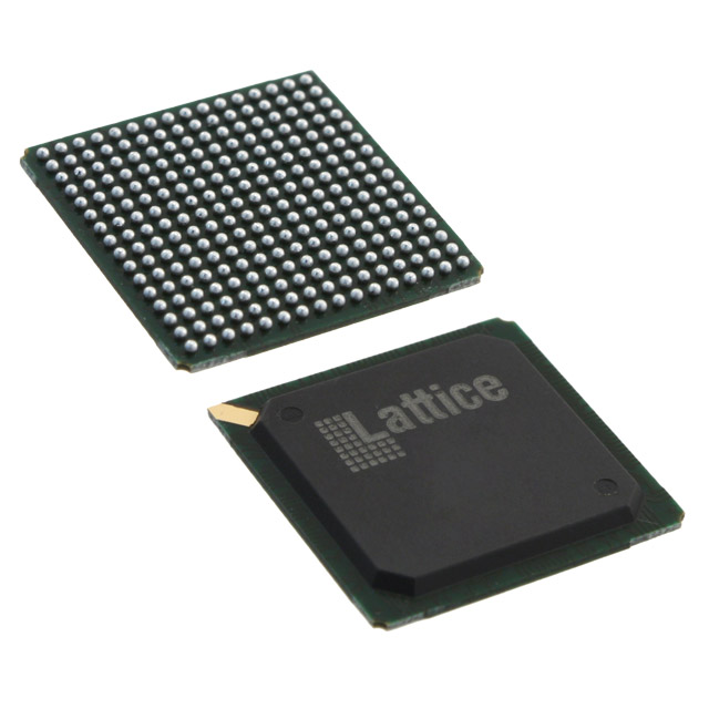
Lattice Semiconductor Corporation LCMXO2-7000HC-4TG144I


- Part Number:
LCMXO2-7000HC-4TG144I
- Manufacturer:
- Category:
- RoHs:
 RoHS Compliant
 - Datasheet:
 LCMXO2-7000HC-4TG144I_Datesheet
 - Description:
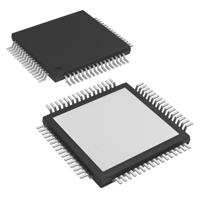
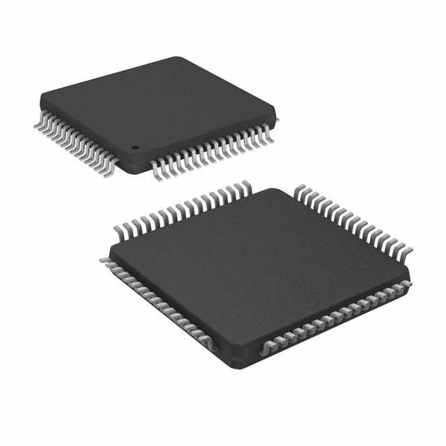
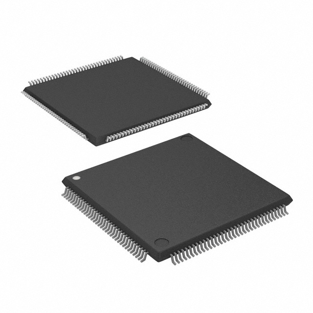
IC FPGA 114 I/O 144TQFP
- In stock 112

LCMXO2-7000HC-4TG144I Model Information
Basic Information
- Device Family: MachXO2
- Model: LCMXO2-7000HC-4TG144I
- Manufacturer: Lattice Semiconductor Corp.
- Ordering Information:LUTs: 6864Supply Voltage: 2.5 V / 3.3 VGrade: IndustrialPackage: TQFP 144Leads: 144Temperature Range: -40°C to 100°CSpeed Grade: -4 (Fastest for Industrial Grade)
Features
- Flexible Logic Architecture: High-density programmable logic with 6864 LUT4s.
- Ultra Low Power: Advanced 65 nm low power process, programmable low swing differential I/Os, stand-by mode and other power saving options.
- Embedded and Distributed Memory: Up to 240 kbits sysMEM™ Embedded Block RAM, up to 54 kbits Distributed RAM.
- On-Chip User Flash Memory: Up to 256 kbits of User Flash Memory, 100,000 write cycles, accessible through WISHBONE, SPI, I2C and JTAG interfaces.
- Pre-Engineered Source Synchronous I/O: DDR registers in I/O cells, dedicated gearing logic, 7:1 Gearing for Display I/Os.
- High Performance, Flexible I/O Buffer: Programmable sysIO™ buffer supports wide range of interfaces.
- Flexible On-Chip Clocking: Eight primary clocks, up to two edge clocks for high-speed I/O interfaces, up to two analog PLLs per device.
- Non-volatile, Infinitely Reconfigurable: Instant-on, single-chip secure solution, programmable through JTAG, SPI or I2C.
- Enhanced System Level Support: On-chip hardened functions, unique TraceID for system tracking, one-time programmable (OTP) mode.
- Broad Range of Package Options: TQFP, WLCSP, ucBGA, csBGA, caBGA, ftBGA, fpBGA, QFN package options.
Electrical Characteristics
- Power Supply Voltage (VCC): 2.5 V / 3.3 V
- I/O Driver Supply Voltage (VCCIO): 1.2 V to 3.3 V
- Junction Temperature (TJ): -40°C to 100°C
- Static Supply Current:Core Power Supply (ICC): 12.87 mA (typical)I/O Bank Power Supply (ICCIO): 0 mA (per bank)
- Programming and Erase Flash Supply Current:Core Power Supply (ICC): 18.3 mA (typical)I/O Bank Power Supply (ICCIO): 0 mA (per bank)
Pin Configuration
- General Purpose I/O per Bank:Bank 0: 27Bank 1: 29Bank 2: 29Bank 3: 9Bank 4: 10Bank 5: 10
- Differential I/O per Bank:Bank 0: 14Bank 1: 14Bank 2: 14Bank 3: 4Bank 4: 5Bank 5: 5
- Dual Function I/O: 37
- High-speed Differential I/O: 9 (Bank 0)
- Gearboxes:Number of 7:1 or 8:1 Output Gearbox Available (Bank 0): 9Number of 7:1 or 8:1 Input Gearbox Available (Bank 2): 14
- DQS Groups: 2 (Bank 1)
Supported Standards
- Single-Ended Interfaces:LVCMOS 3.3: VCCIO = 3.3 V, VIL Max. = 3.135 V, VIH Min. = 3.6 V, VOL Max. (V) = 0.4 VCCIO – 0.4 V, VOH Min. (V) = 0.2 VCCIO – 0.2 V, IOL Max. (mA) = 8, IOH Max. (mA) = -8LVCMOS 2.5: VCCIO = 2.5 V, VIL Max. = 0.7 VCCIO, VIH Min. = 1.7 V, VOL Max. (V) = 0.4 VCCIO – 0.4 V, VOH Min. (V) = 0.2 VCCIO – 0.2 V, IOL Max. (mA) = 8, IOH Max. (mA) = -8LVCMOS 1.8: VCCIO = 1.8 V, VIL Max. = 0.35 VCCIO, VIH Min. = 0.65 VCCIO, VOL Max. (V) = 0.4 VCCIO – 0.4 V, VOH Min. (V) = 0.2 VCCIO – 0.2 V, IOL Max. (mA) = 8, IOH Max. (mA) = -8LVCMOS 1.5: VCCIO = 1.5 V, VIL Max. = 0.35 VCCIO, VIH Min. = 0.65 VCCIO, VOL Max. (V) = 0.4 VCCIO – 0.4 V, VOH Min. (V) = 0.2 VCCIO – 0.2 V, IOL Max. (mA) = 8, IOH Max. (mA) = -8LVCMOS 1.2: VCCIO = 1.2 V, VIL Max. = 0.35 VCCIO, VIH Min. = 0.65 VCCIO, VOL Max. (V) = 0.4 VCCIO – 0.4 V, VOH Min. (V) = 0.2 VCCIO – 0.2 V, IOL Max. (mA) = 4, IOH Max. (mA) = -4LVTTL: VCCIO = 3.3 V, VIL Max. = 0.8 V, VIH Min. = 2.0 V, VOL Max. (V) = 0.4 VCCIO – 0.4 V, VOH Min. (V) = 0.2 VCCIO – 0.2 V, IOL Max. (mA) = 24, IOH Max. (mA) = -24PCI3: VCCIO = 3.3 V, VIL Max. = 0.8 V, VIH Min. = 2.0 V, VOL Max. (V) = 0.4 VCCIO – 0.4 V, VOH Min. (V) = 0.2 VCCIO – 0.2 V, IOL Max. (mA) = 24, IOH Max. (mA) = -24
- Differential Interfaces:SSTL25 Class I: VCCIO = 2.5 V, VIL Max. = VREF – 0.18 V, VIH Min. = VREF + 0.18 V, VOL Max. (V) = 0.54 VCCIO - 0.62 V, VOH Min. (V) = 0.40 VCCIO - 0.40 V, IOL Max. (mA) = 8, IOH Max. (mA) = -8SSTL25 Class II: VCCIO = 2.5 V, VIL Max. = VREF – 0.18 V, VIH Min. = VREF + 0.18 VSSTL18 Class I: VCCIO = 1.8 V, VIL Max. = VREF – 0.125 V, VIH Min. = VREF + 0.125 V, VOL Max. (V) = 0.40 VCCIO - 0.40 V, VOH Min. (V) = 0.40 VCCIO - 0.40 V, IOL Max. (mA) = 8
Purchase
No need to register to order from JMChip Electronics, but signing in lets you track your order like a pro. Give it a try for a smoother shopping ride.
Means
Easy peasy! Pay your way with PayPal, Credit Card, or wire transfer in USD. We've got you covered.
RFQ(Request for Quotations)
Get the freshest prices and stock updates by asking for a quote! Our sales team will shoot you an email within a day. It's that simple.
IMPORTANT NOTICE
1. Look out for your order details in your inbox! (If it's missing, check the spam folder just in case.)
2. Our sales manager will double-check the order and keep you posted on any price or stock changes. No worries, we've got you covered.

Shipping Rate
We ship orders once a day around 5 p.m., except Sunday. Once shipped, the estimated delivery time depends on the courier company you choose, usually 5-7 working days.

Shipping Methods
We provide DHL, FedEx, UPS, EMS, SF Express, and Registered Air Mail international shipping.


Payment
You can pay the orders on the website directly or pay by wire transfer offline. We support: Paypal、VISA、Credit Card.


Lattice Semiconductor Corporation
Lattice Semiconductor Corporation
Lattice Semiconductor Corporation
Lattice Semiconductor Corporation

Lattice Semiconductor Corporation