
Micron Technology Inc. MT40A2G16TBB-062E:F


- Part Number:
MT40A2G16TBB-062E:F
- Manufacturer:
- Category:
- RoHs:
 Non-RoHS Compliant
 - Datasheet:
- Description:
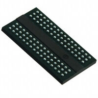
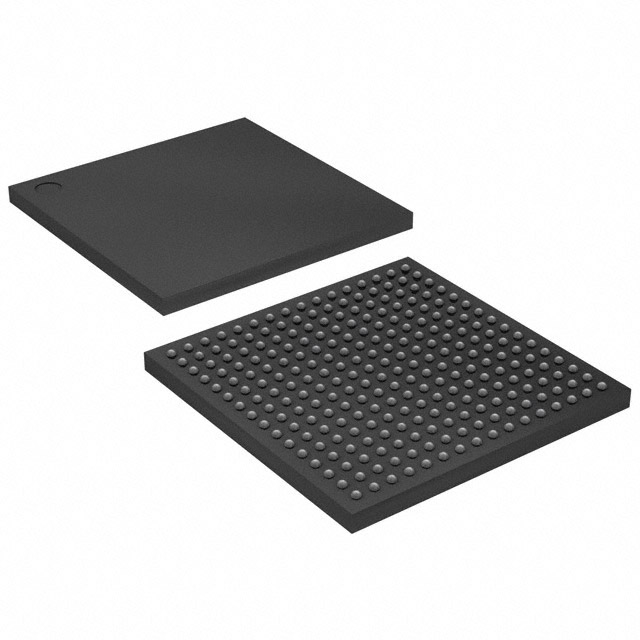
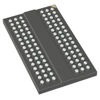
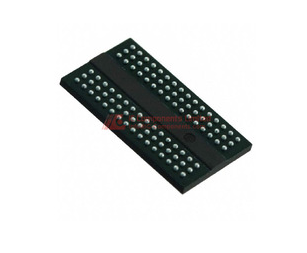
IC DRAM 32GBIT PARALLEL 96FBGA
- In stock 0

MT40A2G16TBB‑062E:F Datasheet Summary
1. Basic Information
- Part Number: MT40A2G16TBB‑062E:F
- Manufacturer: Micron Technology, Inc.
- Device Type: 32Gb (4GB) x16 TwinDie™ Single‑Rank DDR4 SDRAM
- Die Configuration: Two 16Gb x8 dies combined into one x16 device
- Organization: 128 Meg x 16 x 16 Banks x 1 Rank
- Speed Grade: DDR4‑3200 (062E)
- Package: 96‑ball FBGA (7.5 mm × 13 mm × 1.2 mm), Rev F (TBB), Pb‑free
- Voltage: VDD = VDDQ = 1.2V (1.14V – 1.26V)
- Temperature: Commercial (0°C ≤ TC ≤ 95°C)
- Revision: Rev B (document), Die Rev F (TBB package)
- Document: CCM005‑1406124318‑10461, Rev B (12/21)
2. Key Features
- TwinDie architecture: two x8 16Gb dies merged to x16 width
- Single‑rank, 16 banks total (4 banks per bank group)
- 1.2V core and I/O; VDDQ‑terminated I/O
- JEDEC standard pinout; low‑profile package
- Extra ZQ calibration pins (UZQ, LZQ) for faster calibration
- BG1 bank‑group address for x8 die addressing
- Self‑refresh (standard)
- Robust ESD and latch‑up protection
- Parity, DBI, ALERT_n, RESET_n support
3. Addressing & Timing
3.1 Address Map
- Bank Group: BG[1:0]
- Bank Address: BA[1:0]
- Row Address: A[16:0] (128K rows)
- Column Address: A[9:0] (1K columns)
- Page Size: 1KB per bank
3.2 Key Timing (DDR4‑3200, ‑062E)
- Data Rate: 3200 MT/s
- CL‑tRCD‑tRP: 22‑22‑22
- tAA (min): 13.75 ns
- tRCD (min): 13.75 ns
- tRP (min): 13.75 ns
- Cycle Time: 0.625 ns
4. Refresh Requirements
- 0°C – 85°C: 8192 cycles / 64 ms
- 85°C – 95°C: 8192 cycles / 32 ms (2× refresh)
5. Electrical Specifications
5.1 Supply Voltage
- VDD, VDDQ: 1.14V – 1.26V (nominal 1.2V)
- VPP: 2.5V typical (per DDR4 standard)
5.2 Leakage Currents
- Input Leakage (II): ±4 μA max
- VREF Leakage (IVREF): ±4 μA max
- ZQ Pin Leakage (IZQ): –50 to 10 μA
- TEN Pin Leakage (ITEN): –12 to 20 μA
- DQ Output Leakage (IOZPD/IOZPU): ±10 / –50 μA max
5.3 Thermal Characteristics (Rev F TBB)
- Operating Case Temp (TC): 0°C to 95°C
- θJA (0 m/s, low‑conductivity substrate): 48.7°C/W
- θJA (1 m/s): 36.9°C/W
- θJA (2 m/s): 32.4°C/W
- θJC: 2.6°C/W
5.4 Package Electrical
- Zpkg (DQ/DQS): 35 – 60 Ω
- Package Delay (TdIO): 60 – 120 ps
- Lpkg (DQ/DQS): ≤5.5 nH
- Cpkg (DQ/DQS): ≤4 pF
- Zpkg (CMD/ADDR/CTRL): 30 – 70 Ω
- Zpkg (CLK): 30 – 60 Ω
6. Current Specifications (Rev F, 0°C ≤ TC ≤ 85°C)
Combined current for two dies; values for DDR4‑3200:
- ICCD0: 140 mA
- ICPP0: 8 mA
- ICCD1: 168 mA
- ICCD4R (read): 386 mA
- ICCD4W (write): 282 mA
- ICCD5R: 136 mA
- ICCD7: 400 mA
- ICPP7: 26 mA
- ICCD8: 72 mA
7. Pin Summary
- DQ: LDQ[7:0], UDQ[7:0] (16‑bit data)
- DQS: LDQS_t/LDQS_c, UDQS_t/UDQS_c
- DM/DBI: LDM_n/LDBI_n, UDM_n/UDBI_n
- ZQ: UZQ, LZQ (dual calibration)
- CLK: CK_t, CK_c
- CMD/ADDR: CS_n, RAS_n/A16, CAS_n/A15, WE_n/A14, A[16:0], BA[1:0], BG[1:0]
- Control: CKE, ODT, ACT_n, A10/AP, A12/BC_n
- Misc: RESET_n, ALERT_n, PAR, TEN, VREFCA
- Power: VDD, VDDQ, VSS, VSSQ, VPP
8. Functional Description
- TwinDie x16 uses two x8 dies in parallel; control signals shared
- Separate upper/lower DQ, DQS, DM, ZQ for byte lanes
- Connectivity Test Mode: parallel logic matching two monolithic x8
- Internal ECC, DLL, ODT, refresh management
- Supports DBI, CA parity, write CRC, gear down, and DLL off modes
9. Absolute Maximum Ratings
- Voltage (VDD/VDDQ/VPP): –0.3V to 1.5V / 1.5V / 3.0V
- Input Voltage: –0.3V to VDDQ + 0.3V
- Storage Temperature: –55°C to 150°C
- ESD: HBM ±2kV, MM ±200V, CDM ±500V (per Micron standard)
10. Important Notes
- Not intended for automotive use unless designated automotive grade
- Not authorized for critical applications (life support, safety) without robust system safeguards
- Specifications subject to change without notice
- Derate currents above 85°C and for advanced features (parity, DBI, CRC)
Purchase
No need to register to order from JMChip Electronics, but signing in lets you track your order like a pro. Give it a try for a smoother shopping ride.
Means
Easy peasy! Pay your way with PayPal, Credit Card, or wire transfer in USD. We've got you covered.
RFQ(Request for Quotations)
Get the freshest prices and stock updates by asking for a quote! Our sales team will shoot you an email within a day. It's that simple.
IMPORTANT NOTICE
1. Look out for your order details in your inbox! (If it's missing, check the spam folder just in case.)
2. Our sales manager will double-check the order and keep you posted on any price or stock changes. No worries, we've got you covered.

Shipping Rate
We ship orders once a day around 5 p.m., except Sunday. Once shipped, the estimated delivery time depends on the courier company you choose, usually 5-7 working days.

Shipping Methods
We provide DHL, FedEx, UPS, EMS, SF Express, and Registered Air Mail international shipping.


Payment
You can pay the orders on the website directly or pay by wire transfer offline. We support: Paypal、VISA、Credit Card.


Micron Technology Inc.

Micron Technology Inc.
Micron Technology Inc.

Micron Technology Inc.
Micron Technology Inc.
Micron Technology Inc.

Micron Technology Inc.

Micron Technology Inc.
Micron Technology Inc.
Micron Technology Inc.

Micron Technology Inc.
Micron Technology Inc.