
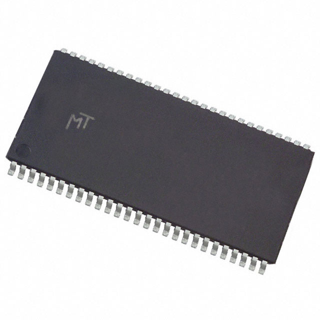
Micron Technology Inc. MT48LC16M16A2P-7E IT:G


- Part Number:
MT48LC16M16A2P-7E IT:G
- Manufacturer:
- Category:
- RoHs:
 RoHS Compliant
 - Datasheet:
 MT48LC16M16A2P-7E IT:G_Datesheet
 - Description:
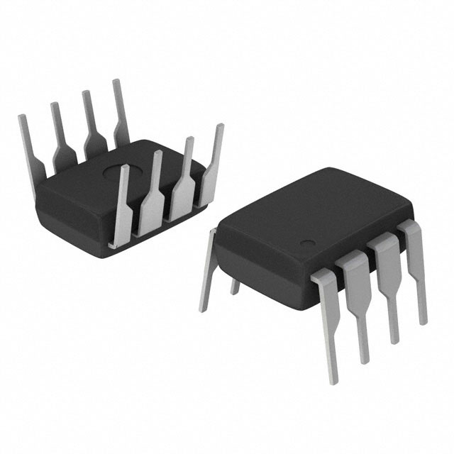
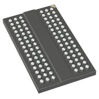
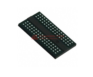
SDRAM Memory IC 256Mbit Parallel 133 MHz 5.4 ns 54-TSOP II
- In stock 0

Information of MT48LC16M16A2P-7E IT:G SDR SDRAM
Basic Overview
- Product Type: 256Mb (4 Meg x 16 x 4 banks) Synchronous Dynamic Random-Access Memory (SDR SDRAM)
- Manufacturer: Micron Technology, Inc.
- Document Reference: 256Mb_sdr.pdf (Rev. W, 05/15 EN)
- Core Function: High-speed data storage with synchronous interface, supporting burst read/write operations for industrial applications
- Key Features: PC133-compliant, 4 internal banks, programmable burst lengths (1/2/4/8/full page), auto/self refresh modes, LVTTL-compatible, single 3.3V ±0.3V supply
- Key Identifiers:
Core Specifications
1. Memory Configuration
| Parameter | Specification |
|---|---|
| Total Capacity | 256Mb (32MB) |
| Organization | 4 Meg x 16 bits x 4 internal banks |
| Row Address | 8K (A[12:0]) |
| Column Address | 512 (A[8:0]) |
| Bank Address | 4 (BA[1:0]) |
| Refresh Count | 8192 cycles |
| Refresh Period | 64 ms (industrial temperature range) |
2. Electrical Characteristics
Absolute Maximum Ratings
| Parameter | Min | Max | Unit |
|---|---|---|---|
| Supply Voltage (VDD/VDDQ) | -1.0 | 4.6 | V |
| Input/Output Voltage (VIN/VIO) | -1.0 | 4.6 | V |
| Storage Temperature (TSTG) | -55 | 150 | °C |
| Power Dissipation | - | 1 | W |
Recommended Operating Conditions
| Parameter | Min | Typ | Max | Unit |
|---|---|---|---|---|
| Supply Voltage (VDD/VDDQ) | 3.0 | 3.3 | 3.6 | V |
| Input High Voltage (VIH) | 2.0 | - | VDD+0.3 | V |
| Input Low Voltage (VIL) | -0.3 | - | 0.8 | V |
| Output High Voltage (VOH) | 2.4 | - | - | V (IOUT=-4mA) |
| Output Low Voltage (VOL) | - | - | 0.4 | V (IOUT=4mA) |
| Operating Temperature (TA) | -40 | - | 85 | °C |
| Junction Temperature (TJ) | -40 | - | 95 | °C |
| Case Temperature (TC) | -40 | - | 90 | °C |
Key AC Timing Parameters (-7E Speed Grade, CL=2)
| Parameter | Symbol | Min | Max | Unit |
|---|---|---|---|---|
| Clock Cycle Time | tCK | 7.5 | - | ns |
| CAS Latency (CL=2) | tAC(2) | - | 5.4 | ns |
| Row Address to Column Address Delay | tRCD | 15 | - | ns |
| Precharge Time | tRP | 15 | - | ns |
| Active to Active Command Period | tRC | 60 | - | ns |
| Refresh Period | tREF | - | 64 | ms |
| Refresh Cycle Time | tRFC | 66 | - | ns |
| Write Recovery Time | tWR | 7 | - | ns (1 CLK + 7ns) |
3. Power Consumption (Revision G, TA=25°C, VDD=3.3V)
| Parameter | Condition | Max | Unit |
|---|---|---|---|
| Operating Current (IDD1) | Active mode, burst=2, read/write | 100 | mA |
| Standby Current (IDD2) | Power-down mode, all banks idle | 2.5 | mA |
| Active Standby Current (IDD3) | CKE=HIGH, CS#=HIGH, no accesses | 35 | mA |
| Page Burst Current (IDD4) | All banks active, page burst | 100 | mA |
| Auto Refresh Current (IDD5) | tRFC=MIN | 150 | mA |
| Self Refresh Current (IDD7) | Standard self refresh | 3 | mA |
| Low-Power Self Refresh Current (IDD7L) | Optional low-power mode | 1.5 | mA |
4. Thermal Characteristics (54-pin TSOP II, Revision G)
| Parameter | Condition | Value | Unit |
|---|---|---|---|
| Junction-to-Ambient Thermal Resistance (θJA) | Airflow=0 m/s, low conductivity substrate | 122.3 | °C/W |
| Airflow=1 m/s, low conductivity substrate | 105.6 | °C/W | |
| Airflow=2 m/s, low conductivity substrate | 98.1 | °C/W | |
| Junction-to-Board Thermal Resistance (θJB) | Low conductivity substrate | 89.5 | °C/W |
| Junction-to-Case Thermal Resistance (θJC) | Low conductivity substrate | 20.7 | °C/W |
Functional Details
1. Key Operational Modes
Burst Operation
- Burst Lengths: Programmable via mode register (1, 2, 4, 8, or full page)
- Burst Types: Sequential or interleaved (selectable via mode register)
- Write Burst Mode: Programmed burst length (default) or single-location access (configurable)
Refresh Modes
- Auto Refresh: 8192 cycles every 64 ms, initiated by external command
- Self Refresh: Low-power mode with internal clocking (retains data without external clock), not supported on automotive variants
- Refresh Addressing: Internal refresh counter generates row addresses automatically
Power-Saving Modes
- Power-Down Mode: Activated via CKE=LOW (precharge power-down for idle banks; active power-down for banks with open rows)
- Clock Suspend: Freezes internal logic during burst access when CKE=LOW
2. Mode Register Configuration
Programmed via LOAD MODE REGISTER command, defining operation parameters:
| Bit Field | Function | Options |
|---|---|---|
| M[2:0] | Burst Length | 000=1, 001=2, 010=4, 011=8, 111=Full Page |
| M3 | Burst Type | 0=Sequential, 1=Interleaved |
| M[6:4] | CAS Latency | 010=2 (for -7E speed grade) |
| M[8:7] | Operating Mode | 00=Standard (only supported option) |
| M9 | Write Burst Mode | 0=Programmed Burst Length, 1=Single Access |
| M[12:10] | Reserved | Must be set to 0 |
3. Command Set
Key commands supported (synchronous to positive clock edge):
- ACTIVE: Select bank and activate row
- READ/WRITE: Initiate burst read/write (supports auto precharge via A10)
- PRECHARGE: Deactivate row (single bank or all banks)
- AUTO REFRESH/SELF REFRESH: Trigger refresh operations
- LOAD MODE REGISTER: Configure operational parameters
- BURST TERMINATE: Truncate ongoing burst operations
- NOP/COMMAND INHIBIT: Idle or disable command execution
Package and Pin Configuration
1. Package Specifications (54-pin TSOP II "P" Suffix)
| Parameter | Min | Max | Unit |
|---|---|---|---|
| Body Length | 22.22 | 22.42 | mm |
| Body Width | 10.16 | 11.76 | mm |
| Package Height | - | 1.2 | mm |
| Lead Pitch | - | 0.65 | mm |
| Lead Width | 0.19 | 0.30 | mm |
| Lead Finish | 90% Sn / 10% Pb (standard) |
2. Key Pin Functions (Top View)
| Pin Group | Pins | Function |
|---|---|---|
| Power | VDD (Multiple pins), VDDQ (Multiple pins) | Core supply (3.3V), DQ supply (3.3V) |
| Ground | VSS (Multiple pins), VSSQ (Multiple pins) | Core ground, DQ ground |
| Data I/O | DQ[15:0] | 16-bit data bus |
| Data Mask | DQML, DQMH | Input/output mask (low=enable, high=mask) |
| Address | A[12:0], BA[1:0] | Row/column address, bank address |
| Control | CLK, CKE | Clock (synchronizes all signals), Clock Enable |
| Command | CS#, RAS#, CAS#, WE# | Chip Select, Row Address Strobe, Column Address Strobe, Write Enable |
| NC | Multiple pins | No connection (leave unconnected) |
Application Guidelines
1. Initialization Sequence
- Simultaneously apply VDD and VDDQ, provide stable CLK.
- Wait 100μs, applying NOP/COMMAND INHIBIT commands.
- Issue PRECHARGE ALL command (A10=HIGH).
- Wait tRP (15 ns), then issue 2 AUTO REFRESH commands (wait tRFC=66 ns between commands).
- Load Mode Register (program burst length, CL=2, burst type, etc.).
- Wait tMRD (2 clock cycles) before normal operation.
2. Operational Notes
- Burst Access: Start with ACTIVE command (select bank/row), followed by READ/WRITE (select column; A10 enables auto precharge).
- Refresh Requirements: Issue 8192 AUTO REFRESH commands every 64 ms to retain data.
- Signal Integrity: VDD/VDDQ and VSS/VSSQ must be powered simultaneously; use decoupling capacitors near supply pins.
- Industrial Temperature: Ensure case temperature (TC) does not exceed 90°C during operation; use forced air cooling if needed.
3. Compatibility
- PC133-compliant, compatible with SDR SDRAM controllers supporting 133 MHz clock, CL=2.
- LVTTL-compatible inputs/outputs for seamless interface with industrial microcontrollers/processors.
Ordering and Compliance
| Part Number Element | Meaning |
|---|---|
| MT48LC16M16A2 | Base part (4 Meg x 16 x 4 banks, A2= tWR=2 CLK) |
| P | 54-pin TSOP II (400 mil, off-center parting line) |
| -7E | Speed grade (133 MHz, CL=2, tCK=7.5 ns) |
| IT | Industrial temperature range (-40°C to +85°C) |
| :G | Revision G |
Complementary Variants
- Pb-Free: MT48LC16M16A2BG (54-ball VFBGA) or MT48LC16M16A2PBG (TSOP II Pb-free)
- Automotive: MT48LC16M16A2P-7E AT (–40°C to +105°C, 16 ms refresh)
- Different Speeds: -6A (167 MHz), -75 (133 MHz, CL=3)
Purchase
No need to register to order from JMChip Electronics, but signing in lets you track your order like a pro. Give it a try for a smoother shopping ride.
Means
Easy peasy! Pay your way with PayPal, Credit Card, or wire transfer in USD. We've got you covered.
RFQ(Request for Quotations)
Get the freshest prices and stock updates by asking for a quote! Our sales team will shoot you an email within a day. It's that simple.
IMPORTANT NOTICE
1. Look out for your order details in your inbox! (If it's missing, check the spam folder just in case.)
2. Our sales manager will double-check the order and keep you posted on any price or stock changes. No worries, we've got you covered.

Shipping Rate
We ship orders once a day around 5 p.m., except Sunday. Once shipped, the estimated delivery time depends on the courier company you choose, usually 5-7 working days.

Shipping Methods
We provide DHL, FedEx, UPS, EMS, SF Express, and Registered Air Mail international shipping.


Payment
You can pay the orders on the website directly or pay by wire transfer offline. We support: Paypal、VISA、Credit Card.


Micron Technology Inc.

Micron Technology Inc.
Micron Technology Inc.

Micron Technology Inc.
Micron Technology Inc.
Micron Technology Inc.

Micron Technology Inc.

Micron Technology Inc.
Micron Technology Inc.
Micron Technology Inc.

Micron Technology Inc.
Micron Technology Inc.