
Micron Technology Inc. MT53E256M32D2DS-053 WT:B


- Part Number:
MT53E256M32D2DS-053 WT:B
- Manufacturer:
- Category:
- RoHs:
 Non-RoHS Compliant
 - Datasheet:
- Description:
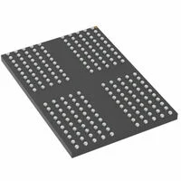
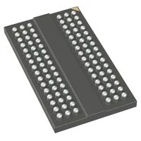
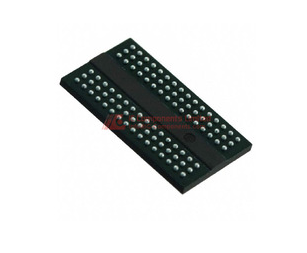
SDRAM - Mobile LPDDR4 Memory IC 8Gbit 1.866 GHz 200-WFBGA (10x14.5)
- In stock 0

MT53E256M32D2DS‑053 WT:B – LPDDR4/LPDDR4X SDRAM Full Specification Summary
1. Basic Device Identification
- Manufacturer: Micron Technology, Inc.
- Part Number: MT53E256M32D2DS‑053 WT:B
- Device Type: Mobile Low‑Power DDR4 (LPDDR4) / LPDDR4X SDRAM
- Density: 8Gb (256M × 32)
- Package: 200‑ball WFBGA (DS code: 10 mm × 14.5 mm × 0.8 mm, Ø0.35 SMD)
- Die Configuration: Dual‑die, dual‑channel, single‑rank (×32 I/O)
- Revision: Rev. I (02/2021)
- RoHS: Compliant (“green” package)
2. Part Number Decoding
- 53: Mobile LPDDR4 SDRAM
- 256M32: 256 Meg × 32 configuration
- D2: 2 dies per package
- DS: 200‑ball WFBGA package
- ‑053: Cycle time 535 ps @ RL = 32/36
- WT: Operating temp. −30°C to +85°C
- :B: Design revision
3. Key Electrical & Timing Parameters
3.1 Power Supplies
- VDD1: 1.70–1.95 V (nominal 1.80 V)
- VDD2: 1.06–1.17 V (nominal 1.10 V)
- VDDQ: 1.06–1.17 V (nominal 1.10 V) or low‑voltage 0.57–0.65 V (nominal 0.60 V for LPDDR4X)
3.2 Speed & Data Rate
- Clock Rate: 1866 MHz
- Data Rate: 3733 Mb/s per pin
- Cycle Time: 535 ps
- Per‑die Bandwidth: Up to 8.5 GB/s
3.3 Latencies (‑053 speed grade)
- Read Latency (RL): 32 (DBI disabled); 36 (DBI enabled)
- Write Latency (WL): Set A = 16; Set B = 30
4. Architecture & Functional Features
- Architecture: 16n prefetch DDR
- Banks: 8 internal banks per channel
- Channels: 2 channels (×16 I/O per channel)
- Burst Length: Programmable BL = 16, 32; on‑the‑fly support
- Command Interface: Single‑data‑rate (SDR) 2‑tick CA bus
- Data Bus: DDR bidirectional; differential DQS per byte lane
- Addressing: BA[2:0], Row[14:0], Column[9:0]
- Page Size: 2048 bytes per channel
5. Key Integrated Features
- On‑chip temperature sensor for self‑refresh rate control
- Partial‑Array Self Refresh (PASR)
- Per‑bank refresh for concurrent operation
- Programmable READ/WRITE latencies (RL/WL)
- Selectable output drive strength
- Programmable on‑die termination (ODT) for CA and DQ buses
- Data Bus Inversion (DBI) and Data Mask (DM)
- Clock‑stop capability
- ZQ calibration for output impedance and termination
- Target Row Refresh (TRR) mode
- Post‑Package Repair (PPR) support
6. Operating Conditions
- Temperature Range: −30°C to +85°C (WT grade)
- Command/Address: Differential clock inputs (CK_t/CK_c)
- Control Signals: CKE, CS_n, RESET_n, ODT_CA
- I/O: DQ[31:0], DQS[3:0]_t/c, DMI[3:0]
- ZQ Calibration: 240 Ω ±1% reference resistor to VDDQ
7. Key Timing & Power Summary
7.1 Power Consumption (IDD, 3733 Mb/s, 85°C)
- Active (IDD4R2): 322 mA (VDD2)
- Active Write (IDD4W2): 265 mA (VDD2)
- Self Refresh (IDD6): 1.0 mA (VDD1), 3.8 mA (VDD2), 0.75 mA (VDDQ)
7.2 Power‑Up & Initialization
- Voltage ramp time (tINIT0): ≤20 ms
- RESET_n LOW after ramp (tINIT1): ≥200 μs
- Stable clock before CKE (tINIT4): ≥5 tCK
- Mode register setup: VREF(CA/DQ), ODT, drive strength, latency
8. Mode Register Highlights
- MR0: Refresh mode, latency type
- MR1: Burst length, read/write preamble/postamble
- MR2: Write leveling, WL/RL selection
- MR3: DBI enable, drive strength, PPR
- MR11: CA and DQ ODT control
- MR12/MR14: VREF(CA) and VREF(DQ) tuning
- MR13: Frequency set point, command bus training
- MR16/MR17: PASR bank/segment masking
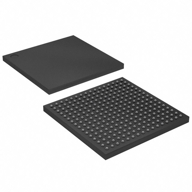
9. Package & Mechanical
- Package Code: DS
- Form Factor: 200‑ball WFBGA
- Dimensions: 10 mm × 14.5 mm × 0.8 mm
- Solder Balls: SAC302 (96.8% Sn, 3.0% Ag, 0.2% Cu)
- Ball Pitch: 0.65 mm typical
10. Command & Operation Summary
- Supported commands: ACTIVATE, READ/WRITE, MASK WRITE, PRECHARGE, REFRESH (all‑bank/per‑bank), SELF REFRESH, MODE REGISTER READ/WRITE, MPC (multipurpose)
- Burst operations: BL16/BL32, seamless/consecutive READ/WRITE
- Power modes: Idle, active, power‑down, self‑refresh
- Training: Command bus, write leveling, read DQ calibration, ZQ calibration
11. Reliability & Compliance
- ESD protection
- Latch‑up immunity
- JEDEC standard compliant
- RoHS‑compliant, halogen‑free (“green”)
Purchase
No need to register to order from JMChip Electronics, but signing in lets you track your order like a pro. Give it a try for a smoother shopping ride.
Means
Easy peasy! Pay your way with PayPal, Credit Card, or wire transfer in USD. We've got you covered.
RFQ(Request for Quotations)
Get the freshest prices and stock updates by asking for a quote! Our sales team will shoot you an email within a day. It's that simple.
IMPORTANT NOTICE
1. Look out for your order details in your inbox! (If it's missing, check the spam folder just in case.)
2. Our sales manager will double-check the order and keep you posted on any price or stock changes. No worries, we've got you covered.

Shipping Rate
We ship orders once a day around 5 p.m., except Sunday. Once shipped, the estimated delivery time depends on the courier company you choose, usually 5-7 working days.

Shipping Methods
We provide DHL, FedEx, UPS, EMS, SF Express, and Registered Air Mail international shipping.


Payment
You can pay the orders on the website directly or pay by wire transfer offline. We support: Paypal、VISA、Credit Card.


Micron Technology Inc.

Micron Technology Inc.
Micron Technology Inc.

Micron Technology Inc.
Micron Technology Inc.
Micron Technology Inc.

Micron Technology Inc.

Micron Technology Inc.
Micron Technology Inc.
Micron Technology Inc.

Micron Technology Inc.
Micron Technology Inc.