
Macronix MX25L3233FM2I-08G


- Part Number:
MX25L3233FM2I-08G
- Manufacturer:
- Category:
- RoHs:
 RoHS Compliant
 - Datasheet:
 MX25L3233FM2I-08G_Datesheet
 - Description:
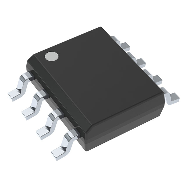
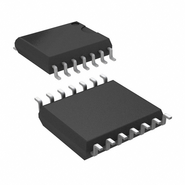
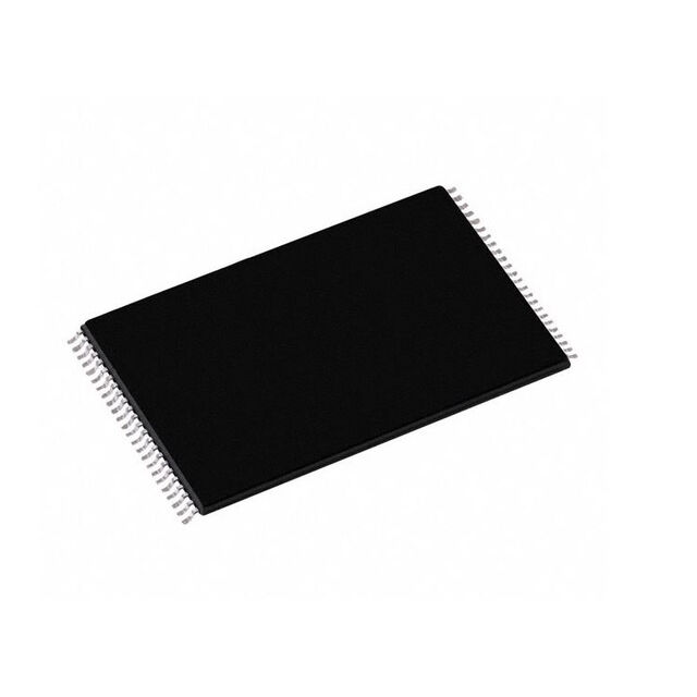
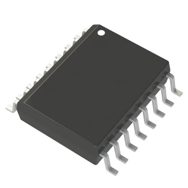
IC FLASH 32MBIT SPI/QUAD 8SOP
- In stock 39,360

MX25L3233FM2I-08G: 3V, 32Mb Serial Flash Memory
General Description
The MX25L3233FM2I-08G is a 3V, 32Mb Serial NOR Flash memory device from Macronix International Co., Ltd. It is designed for high-performance and low-power applications, supporting various serial I/O modes and advanced features.
Key Features
- Memory Density: 32Mb (4,194,304 bytes)
- Operating Voltage: 2.65V to 3.6V
- Clock Frequency: Up to 133 MHz
- Temperature Range: Industrial grade (-40°C to 85°C)
- Package Type: 8-pin SOP (200mil)
- Program/Erase Cycles: Up to 100,000 cycles
- Data Retention: 20 years at 55°C
- Protection Features: Block lock protection, 4K-bit secured OTP, and hardware/software protection modes
- Performance Enhance Mode: XIP (execute-in-place) mode available
Memory Organization
- Structure: 32,768 sectors of 1,024 bytes each
- Blocks:128 blocks of 32,768 bytes (32KB) each64 blocks of 65,536 bytes (64KB) each
- Addressing: 3-byte addresses for up to 16,777,216 bytes (16MB)
Command Set
The MX25L3233FM2I-08G supports a wide range of commands, including:
- Read Operations: Normal read, fast read, dual read, quad read
- Program Operations: Page program, quad page program
- Erase Operations: Sector erase, block erase (32KB, 64KB), chip erase
- Status and Configuration: Read status register, write status register, read configuration register
- Advanced Features: Program suspend/resume, erase suspend/resume, deep power-down mode, burst read
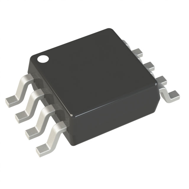
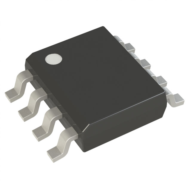
Pin Configuration
8-pin SOP (200mil)
- CS#: Chip Select
- SI/SIO0: Serial Data Input (for 1x I/O)/Serial Data Input & Output (for 2x I/O mode and 4x I/O mode)
- SO/SIO1: Serial Data Output (for 1x I/O)/Serial Data Input & Output (for 2x I/O mode and 4x I/O mode)
- SCLK: Clock Input
- WP#/SIO2: Write Protection Active Low or Serial Data Input & Output (for 4x I/O mode)
- HOLD#/SIO3: To pause the device without deselecting the device or Serial Data Input/Output for 4x I/O mode
- VCC: +3.0V Power Supply
- GND: Ground
Electrical Specifications
- Standby Current (ISB1): 10 uA typical, 50 uA maximum
- Deep Power-Down Current (ISB2): 3 uA typical, 20 uA maximum
- Read Current (ICC1): 2.5 mA typical, 5 mA maximum (50MHz), 10 mA typical, 17 mA maximum (133MHz)
- Program Current (ICC2): 10 mA typical, 15 mA maximum
- Erase Current (ICC4): 10 mA typical, 15 mA maximum
- Input Voltage (VIL, VIH): -0.5V to VCC+0.4V
- Output Voltage (VOL, VOH): VOL ≤ 0.4V, VOH ≥ VCC-0.2V
Timing Specifications
- Clock Frequency (fSCLK): Up to 133 MHz
- Clock High Time (tCH): 9 ns (≤ 50MHz), 45% x (1/fSCLK) ( > 50MHz)
- Clock Low Time (tCL): 9 ns (≤ 50MHz), 45% x (1/fSCLK) ( > 50MHz)
- Clock Rise/Fall Time (tCLCH, tCLCL): 0.1 V/ns
- CS# Active Setup Time (tSLCH): 4 ns
- CS# Not Active Hold Time (tCHSL): 4 ns
- Data In Setup Time (tDVCH): 2 ns
- Data In Hold Time (tCHDX): 3 ns
Operating Conditions
- Ambient Operating Temperature: Industrial grade (-40°C to 85°C)
- Storage Temperature: -65°C to 150°C
- Power-Up/Down: Ensure VCC reaches the minimum level before selecting the device
Ordering Information
- Part Number: MX25L3233FM2I-08G
- Package: 8-pin SOP (200mil)
- Clock Frequency: 133 MHz
- Temperature Range: -40°C to 85°C
Package Dimensions
8-pin SOP (200mil)
- A: 0.10 mm to 1.75 mm
- A1: 0.15 mm typical
- A2: 1.35 mm typical
- b: 0.36 mm typical
- C: 4.77 mm to 5.03 mm
- D: 5.80 mm to 6.20 mm
- E: 3.80 mm to 4.00 mm
- E1: 1.27 mm typical
- e: 0.46 mm to 0.86 mm
- L: 0.85 mm typical
- L1: 1.05 mm typical
- S: 0.54 mm typical
- Θ: 5° to 8°
Purchase
No need to register to order from JMChip Electronics, but signing in lets you track your order like a pro. Give it a try for a smoother shopping ride.
Means
Easy peasy! Pay your way with PayPal, Credit Card, or wire transfer in USD. We've got you covered.
RFQ(Request for Quotations)
Get the freshest prices and stock updates by asking for a quote! Our sales team will shoot you an email within a day. It's that simple.
IMPORTANT NOTICE
1. Look out for your order details in your inbox! (If it's missing, check the spam folder just in case.)
2. Our sales manager will double-check the order and keep you posted on any price or stock changes. No worries, we've got you covered.

Shipping Rate
We ship orders once a day around 5 p.m., except Sunday. Once shipped, the estimated delivery time depends on the courier company you choose, usually 5-7 working days.

Shipping Methods
We provide DHL, FedEx, UPS, EMS, SF Express, and Registered Air Mail international shipping.


Payment
You can pay the orders on the website directly or pay by wire transfer offline. We support: Paypal、VISA、Credit Card.


Macronix
Macronix
Macronix
Macronix
Macronix
Macronix
Macronix
Macronix
Macronix
Macronix
Macronix

Macronix