




 All Products
Nexperia USA Inc. NPS4053GV-Q100H


- Part Number:
NPS4053GV-Q100H
- Manufacturer:
- Category:
- RoHs:
 Non-RoHS Compliant
 - Datasheet:
- Description:
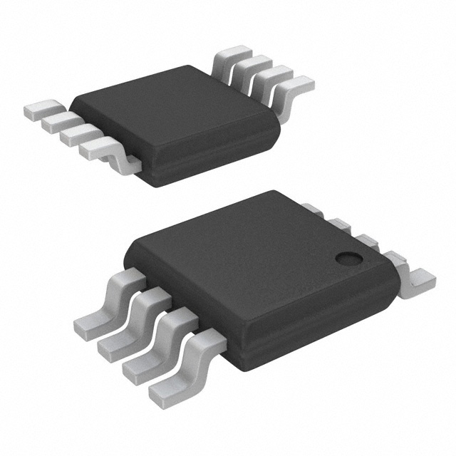
NPS4053GV-Q100/SOT457/SC-74
- In stock 2,530



Full Datasheet Information Summary of NPS4053GV-Q100
Document Basic Info
- Device Full Model: NPS4053GV-Q100 (Suffix H represents tape & reel packaging form)
- Manufacturer: Nexperia
- Datasheet Version: Rev.2, Release Date: 20 October 2023
- Device Definition: 5.5 V, 55 mΩ automotive-grade P-channel load switch with precision adjustable constant current limit
- Automotive Qualification: AEC-Q100 Grade 1, operating temperature range: -40 °C ~ +125 °C
1. Core Product Overview
The NPS4053GV-Q100 is a single-channel power load switch optimized for automotive power distribution, USB hubs and ECU power rails. It supports adjustable current limiting from 110 mA to 2.5 A. When overload or short-circuit occurs, the IC enters constant-current regulation mode to clamp output current. Integrated active reverse voltage protection cuts off the internal MOSFET when VOUT > VIN to avoid backfeeding damage to upstream power sources. An open-drain active-low FLG fault flag pin reports overcurrent, overtemperature and reverse voltage faults to system controllers.
Key built-in advantages: soft-start slew rate control, ILIM pin self-protection, UVLO undervoltage lockout, full ESD robustness and thermal shutdown cycling protection.
2. Key Features & Electrical Benefits
2.1 Voltage & Current Ratings
- Input operating voltage range (VIN): 2.5 V ~ 5.5 V (UVLO rising threshold typical 2.35 V)
- Maximum continuous DC output current (IOUT): 2 A
- Adjustable current limit range: 110 mA ~ 2.5 A, ±6% limit accuracy at 1.2 A
- Current limit calculation formula: \(I_{ILIM}(mA)=\frac{23600}{R_{ILIM}(k\Omega)}\)
- Recommended ILIM resistor range: 9.31 kΩ ~ 210 kΩ (1% tolerance precision resistor)
2.2 On-State Resistance (RDS(on), Typical @25°C)
| Input Voltage | Typical RDS(on) | Max RDS(on) |
|---|---|---|
| 5.5 V | 55 mΩ | 88 mΩ |
| 3.6 V | 65 mΩ | 109 mΩ |
| 2.5 V | 80 mΩ | 140 mΩ |
2.3 Protective Functions
- Constant-Current Overcurrent Protection: Locks output to ILIM threshold under overload/short; FLG pulls low after 8.5 ms deglitch delay
- ILIM Pin Self-Protection: ILIM pin can be shorted to GND or left floating without device damage; shorted ILIM defaults to ~2.46 A limit, floating ILIM defaults to ~110 mA limit
- Active Reverse Voltage Blocking: Turns off power MOSFET when VOUT exceeds VIN by 75 mV for 0.5 μs; FLG triggers after 0.2 ms deglitch
- Thermal Shutdown (OTP): Junction temperature threshold 155 °C, 10 °C thermal hysteresis; auto-retry cycling after cooling, FLG asserts immediately without deglitch
- Undervoltage Lockout (UVLO): Prevents switch turn-on when VIN is below ~2.35 V, 25 mV built-in hysteresis to avoid chattering
- No Reverse Body Diode: No current conduction path from OUT to IN when switch is disabled, eliminates reverse leakage risk
2.4 Soft-Start & Timing Parameters
- Built-in soft-start to suppress inrush current during power-up
- Turn-on time (ton, max): 3 ms
- Turn-off time (toff, max): 3 ms
- Output rise time (tr typical): 0.2–0.3 ms
- Output fall time (tf typical): 0.2 ms
2.5 Quiescent & Leakage Current
- Operating quiescent current (IQ, max): 285 μA (VIN=5.5 V, ON=High, no load)
- Shutdown supply current (ISD, max): 1 μA (ON pin logic low)
- Reverse leakage current (IREV, typical): 150 nA (VIN=0 V, VOUT=5.5 V)
2.6 ESD & Surge Robustness
- HBM ESD: Class 2, >2000 V
- CDM ESD: Class C2a, >500 V
- IEC 61000-4-2 Contact discharge: 8000 V
- IEC 61000-4-2 Air-gap discharge: 15000 V
- UL 62368 safety certification compliant
3. Packaging & Marking Information
3.1 Package Definition of NPS4053GV-Q100
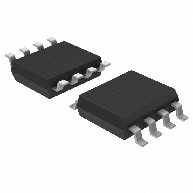
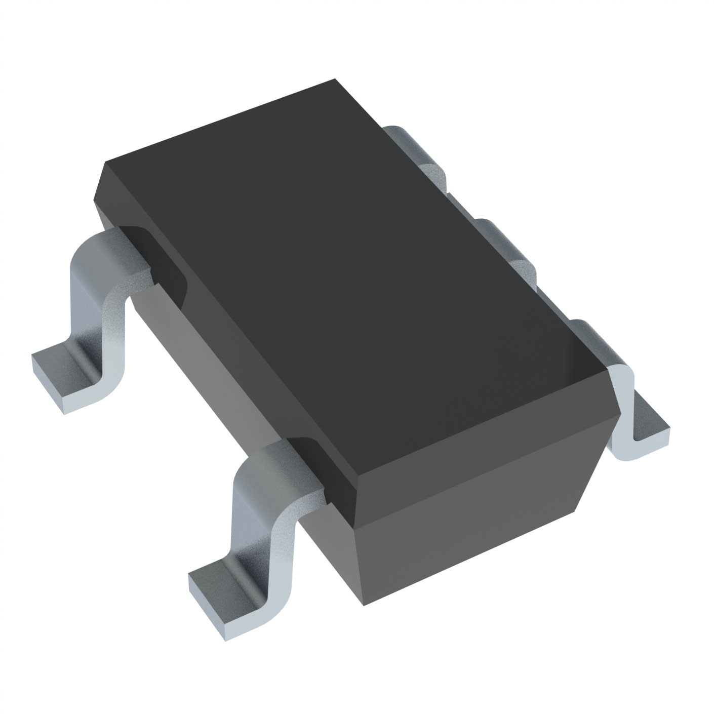
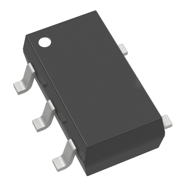
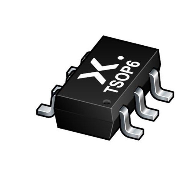
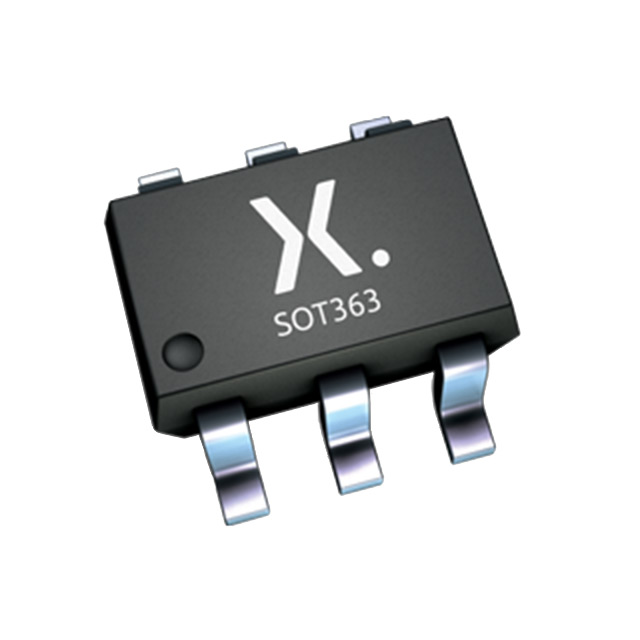
- Package Code: SOT457 (SC-74 / TSOP6)
- Form: 6-lead gull-wing plastic surface-mount package
- Temperature range: -40 °C ~ +125 °C
- Body dimension: 3.1 mm (max length) × 1.7 mm (max width) × 0.8 mm (max height)
- Thermal resistance (θJA): 160 °C/W
- Internal marking code on package: s3
- Packaging suffix H: Tape & Reel SMD packaging
3.2 Alternative Package Reference (NPS4053GH-Q100)
- SOT8044-1 (HWSON6): leadless thermal-enhanced package, 2.0×2.0×0.75 mm, 0.65 mm pin pitch, θJA=63.4 °C/W
4. Pin Assignment & Pin Description (SOT457 TSOP6)
| Pin No. | Symbol | I/O Type | Functional Description |
|---|---|---|---|
| 1 | IN | Power Input | Power supply input; Place ≥0.1 μF ceramic capacitor close to IC between IN and GND |
| 2 | GND | Power Ground | Device common ground, PCB ground connection |
| 3 | ON | Logic Input | Enable pin: Logic HIGH turns on power switch; VIH ≥1.4 V, VIL ≤0.35 V; TTL/CMOS compatible |
| 4 | FLG | Open-Drain Output | Active-low fault indicator; Pull up to VIN via external resistor (100 kΩ typical); Flags overcurrent, OTP, reverse voltage; Max sink current 10 mA |
| 5 | ILIM | Analog Output | Current-limit programming pin; Connect resistor to GND to set ILIM threshold; Max source current 1 mA |
| 6 | OUT | Power Output | Load power output; USB applications require ≥120 μF output capacitor; Other applications sized by transient load demand |
5. Absolute Maximum Ratings (Stress Limits, IEC 60134)
All voltages referenced to GND; exceeding any value causes permanent device damage
| Parameter | Symbol | Min | Max | Unit |
|---|---|---|---|---|
| Input pin voltage | VIN | -0.3 | 6 | V |
| Output pin voltage | VOUT | -0.3 | 6 | V |
| Enable pin voltage | VON | -0.3 | 6 | V |
| ILIM pin voltage | VILIM | -0.3 | 6 | V |
| FLG pin voltage | VFLG | -0.3 | 6 | V |
| IN-OUT differential voltage | VIN-VOUT | -6 | +6 | V |
| FLG sink current | IFLG | 0 | 25 | mA |
| ILIM source current | IILIM | 0 | 1 | mA |
| Junction temperature | TJ | -40 | 150 | °C |
| Storage temperature | TSTG | -65 | 150 | °C |
6. Recommended Operating Conditions
| Parameter | Min | Max | Unit |
|---|---|---|---|
| Input supply voltage VIN | 2.2 | 5.5 | V |
| ON pin logic voltage | 0 | 5.5 | V |
| Continuous output current IOUT | 0 | 2 | A |
| ILIM programming resistor RILIM | 9.31 | 210 | kΩ |
| FLG continuous sink current | 0 | 10 | mA |
| Ambient operating temperature Tamb | -40 | 125 | °C |
7. Typical Application Circuits
7.1 Single Fixed Current Limit Circuit
- Configuration: ILIM pin connected to 15 kΩ resistor to GND, sets ILIM=1.57 A @ VIN=5 V
- Input: 0.1 μF ceramic capacitor from IN to GND
- FLG pin pulled up to VIN via 100 kΩ resistor for fault reporting to MCU
- USB load requirement: ≥120 μF output capacitor at OUT pin
7.2 Two-Level Dynamic Current Limit Circuit
Dual Current Limit Circuit
- Two parallel resistors (20 kΩ each) with a MOSFET switch to toggle limit thresholds
- Threshold 1 (MOSFET OFF): 1.18 A; Threshold 2 (MOSFET ON): 2.36 A
7.3 Auto-Retry Overcurrent Recovery Circuit
- FLG pin shorted to ON pin with RC timing network (10 kΩ + 0.1 μF)
- Operation logic: Overcurrent pulls FLG low to disable switch; Fault clears, FLG rises to re-enable automatically, retry period determined by RC time constant
8. Main Application Scenarios
- Automotive ECU internal power distribution rails
- Automotive USB ports / USB hubs
- Precision adjustable constant-current limiting circuits
- Low-voltage 2.5 V–5.5 V load power management with short-circuit protection
9. PCB Layout & Thermal Design Guidelines
9.1 Layout Rules
- Place input 0.1 μF MLCC capacitor as close as possible between IN and GND pins to minimize parasitic inductance
- Use wide, short copper traces for IN, OUT and GND power paths to reduce IR drop and inductance
- Output bulk capacitor positioned adjacent to OUT and GND pins, critical for USB load transient stability
- Separate analog small-signal traces (ON, FLG, ILIM) from high-current power traces to avoid noise coupling
9.2 Thermal Calculation Formula
Maximum allowable power dissipation:
\(P_{D(MAX)}=\frac{T_{J(MAX)}-T_{amb}}{\theta_{JA}}\)
- TJ(MAX)=125 °C (normal continuous operation limit)
- θJA=160 °C/W for SOT457 (NPS4053GV-Q100)
- Improve thermal performance by expanding GND copper area under the package
10. Functional Block Diagram Overview
Internal Functional Block Diagram
Internal modules: Power Switch & Driver, Current Sense, Current Limit Regulation, OTP Thermal Detection, Switch Control Logic, FLG Fault Output Control, Internal Supply Regulator, TRCB transient protection circuit.
Purchase
No need to register to order from JMChip Electronics, but signing in lets you track your order like a pro. Give it a try for a smoother shopping ride.
Means
Easy peasy! Pay your way with PayPal, Credit Card, or wire transfer in USD. We've got you covered.
RFQ(Request for Quotations)
Get the freshest prices and stock updates by asking for a quote! Our sales team will shoot you an email within a day. It's that simple.
IMPORTANT NOTICE
1. Look out for your order details in your inbox! (If it's missing, check the spam folder just in case.)
2. Our sales manager will double-check the order and keep you posted on any price or stock changes. No worries, we've got you covered.

Shipping Rate
We ship orders once a day around 5 p.m., except Sunday. Once shipped, the estimated delivery time depends on the courier company you choose, usually 5-7 working days.

Shipping Methods
We provide DHL, FedEx, UPS, EMS, SF Express, and Registered Air Mail international shipping.


Payment
You can pay the orders on the website directly or pay by wire transfer offline. We support: Paypal、VISA、Credit Card.




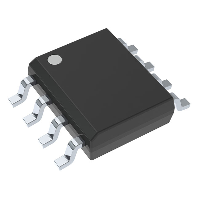

Nexperia USA Inc.
Nexperia USA Inc.
Nexperia USA Inc.
Nexperia USA Inc.
Nexperia USA Inc.
Nexperia USA Inc.
Nexperia USA Inc.
Nexperia USA Inc.
Nexperia USA Inc.
Nexperia USA Inc.
Nexperia USA Inc.
Nexperia USA Inc.


