
Nexperia USA Inc. 74ALVC162836ADGG:1


- Part Number:
74ALVC162836ADGG:1
- Manufacturer:
- Category:
- RoHs:
 RoHS Compliant
 - Datasheet:
 74ALVC162836ADGG:1_Datesheet
 - Description:
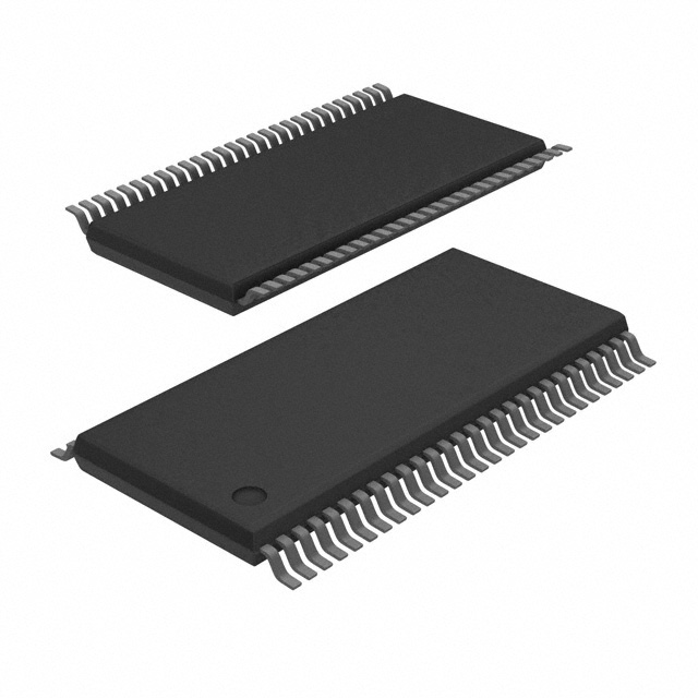
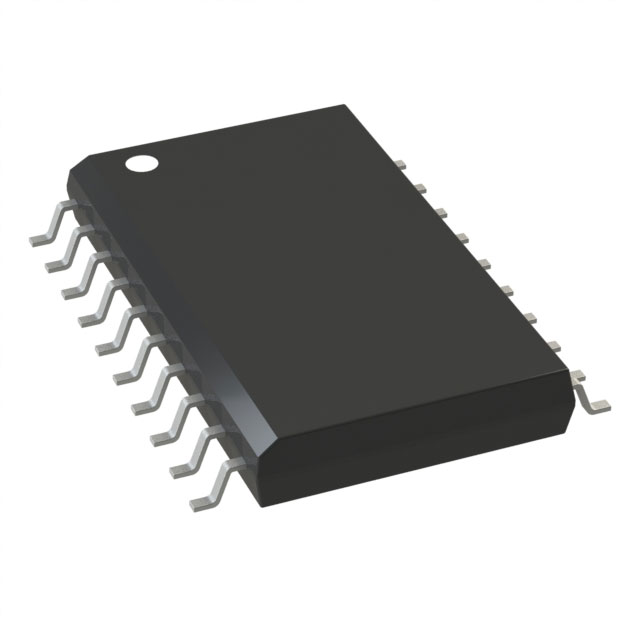
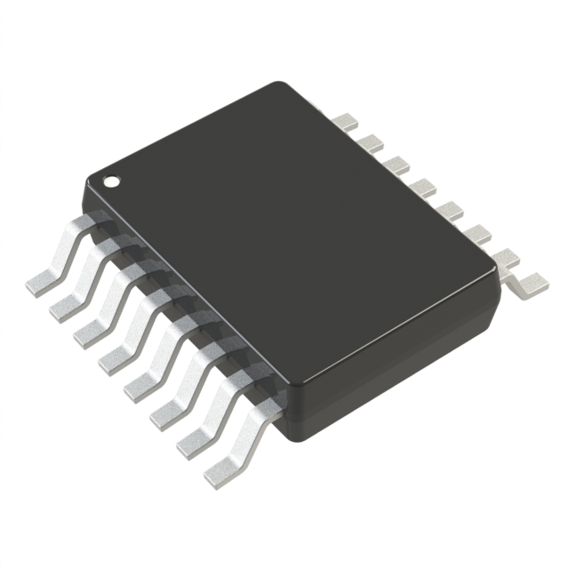
IC UNIV BUS DVR 20BIT 56TSSOP
- In stock 0

74ALVC162836ADGG:1 Datasheet Summary
General Description
The 74ALVC162836ADGG:1 is a 20-bit registered driver with inverted register enable and 30Ω termination resistors. It features a 3-state output and is designed for universal bus driving applications. The data flow is controlled by output enable (OE), latch enable (LE), and clock inputs.
Features and Benefits
- Wide supply voltage range: 1.2V to 3.6V
- CMOS low-power consumption
- Direct interface with TTL levels
- Current drive capability of ±12mA at 3.0V
- MULTIBYTE flow-through standard pin-out architecture
- Low inductance multiple VCC and GND pins for minimum noise and ground bounce
- Output drive capability for 50Ω transmission lines at 85°C
- Integrated 30Ω termination resistors
- Diode clamps to VCC and GND on all inputs
- Input diodes to accommodate strong drivers
- Compliance with JEDEC standards:JESD8-5 (2.3V to 2.7V)JESD8B/JESD36 (2.7V to 3.6V)
- ESD protection:HBM ANSI/ESDA/JEDEC JS-001 exceeds 2000VCDM JESD22-C101E exceeds 1000V
Ordering Information
- Temperature range: -40°C to +85°C
- Package: Plastic thin shrink small outline package (TSSOP56), 56 leads, body width 6.1mm (SOT364-1)
Pinning Information
Pin Configuration
- OE (Pin 1): Output enable input (active LOW)
- LE (Pin 29): Latch enable input (active LOW)
- CP (Pin 56): Clock input
- A1 to A20 (Pins 55, 54, 52, 51, 49, 48, 47, 45, 44, 43, 42, 41, 40, 38, 37, 36, 34, 23, 24, 27): Data inputs
- Y1 to Y20 (Pins 2, 3, 5, 6, 8, 9, 10, 12, 13, 14, 15, 16, 17, 19, 20, 21, 23, 24, 26, 27): Data outputs
- GND (Pins 4, 11, 18, 25, 32, 39, 46, 53): Ground
- Vcc (Pins 7, 22, 35, 50): Supply voltage
- n.c. (Pin 28): No connection
Pin Description
TableCopy
| Symbol | Pin | Description |
|---|---|---|
| A1-A20 | 55,54,52,51,49,48,47,45,44,43,42,41,40,38,37,36,34,23,24,27 | Data inputs |
| Y1-Y20 | 2,3,5,6,8,9,10,12,13,14,15,16,17,19,20,21,23,24,26,27 | Data outputs |
| n.c. | 28 | No connection |
| LE | 29 | Latch enable input (active LOW) |
| OE | 1 | Output enable input (active LOW) |
| CP | 56 | Clock input |
| GND | 4,11,18,25,32,39,46,53 | Ground (0 V) |
| Vcc | 7,22,35,50 | Supply voltage |
Functional Description
The 74ALVC162836ADGG:1 operates as follows:
- When LE is HIGH, the data flow from An to Yn is transparent.
- When LE is HIGH and CP is held at LOW or HIGH, the data is latched.
- On the LOW to HIGH transient of CP, the A data is stored in the register.
- When OE is LOW, the outputs are active.
- When OE is HIGH, the outputs go to the high-impedance OFF-state.
Limiting Values
TableCopy
| Parameter | Conditions | Min | Max | Unit |
|---|---|---|---|---|
| Vcc | Supply voltage | -0.5 | +4.6 | V |
| V | Input voltage | -0.5 | +4.6 | V |
| Vo | Output voltage | -0.5 | Vcc +0.5 | V |
| I_K | Input clamping current (V<0V) | - | -50 | mA |
| I_oK | Output clamping current (Vo>Vcc or Vo<0V) | - | ±50 | mA |
| I | Output current (Vo = 0V to Vcc) | - | ±50 | mA |
| Icc | Supply current | - | 100 | mA |
| I_GND | Ground current | -100 | - | mA |
| T_stg | Storage temperature | -65 | +150 | °C |
| P_tot | Total power dissipation | - | 600 | mW |
Recommended Operating Conditions
TableCopy
| Parameter | Conditions | Min | Typ | Max | Unit |
|---|---|---|---|---|---|
| Vcc | Supply voltage | 1.2 | - | 3.6 | V |
| V | Input voltage | 0 | - | Vcc | V |
| Vo | Output voltage | 0 | - | Vcc | V |
| Tamb | Ambient temperature (operating in free-air) | -40 | - | +85 | °C |
| Δt/ΔV | Input transition rise and fall rate (Vcc = 2.3V to 3.0V) | 0 | - | 20 | ns/V |
| Δt/ΔV | Input transition rise and fall rate (Vcc = 3.0V to 3.6V) | 0 | - | 10 | ns/V |
Static Characteristics
TableCopy
| Parameter | Conditions | Min | Typ | Max | Unit | |
|---|---|---|---|---|---|---|
| VIH | HIGH-level input voltage (VCC = 2.3 V to 2.7 V) | 1.7 | 1.2 | - | V | |
| VIH | HIGH-level input voltage (VCC = 2.7 V to 3.6 V) | 2.0 | 1.5 | - | V | |
| VIL | LOW-level input voltage (VCC = 2.3 V to 2.7 V) | - | 1.2 | 0.7 | V | |
| VIL | LOW-level input voltage (VCC = 2.7 V to 3.6 V) | - | 1.5 | 0.8 | V | |
| VOH | HIGH-level output voltage (VCC = 2.3 V to 3.6 V; IO = -100 μA) | VCC - 0.2 | VCC | - | V | |
| VOH | HIGH-level output voltage (VCC = 2.3 V; IO = -4 mA) | VCC - 0.4 | VCC - 0.11 | - | V | |
| VOH | HIGH-level output voltage (VCC = 2.3 V; IO = -6 mA) | VCC - 0.6 | VCC - 0.17 | - | V | |
| VOH | HIGH-level output voltage (VCC = 2.7 V; IO = -4 mA) | VCC - 0.5 | VCC - 0.09 | - | V | |
| VOH | HIGH-level output voltage (VCC = 2.7 V; IO = -8 mA) | VCC - 0.7 | VCC - 0.19 | - | V | |
| VOH | HIGH-level output voltage (VCC = 3.0 V; IO = -6 mA) | VCC - 0.6 | VCC - 0.13 | - | V | |
| VOH | HIGH-level output voltage (VCC = 3.0 V; IO = -12 mA) | VCC - 1.0 | VCC - 0.27 | - | V | |
| VOL | LOW-level output voltage (VCC = 2.3 V to 3.6 V; IO = 100 μA) | - | GND | 0.20 | V | |
| VOL | LOW-level output voltage (VCC = 2.3 V; IO = 4 mA) | - | 0.07 | 0.40 | V | |
| VOL | LOW-level output voltage (VCC = 2.3 V; IO = 6 mA) | - | 0.11 | 0.55 | V | |
| VOL | LOW-level output voltage (VCC = 2.7 V; IO = 4 mA) | - | 0.06 | 0.40 | V | |
| VOL | LOW-level output voltage (VCC = 2.7 V; IO = 8 mA) | - | 0.13 | 0.60 | V | |
| VOL | LOW-level output voltage (VCC = 3.0 V; IO = 6 mA) | - | 0.09 | 0.55 | V | |
| VOL | LOW-level output voltage (VCC = 3.0 V; IO = 12 mA) | - | 0.19 | 0.80 | V | |
| II | Input leakage current (VCC = 2.3 V to 3.6 V; VI = VCC or GND) | -0.1 | 5 | -0.1 | 10 | μA |
| IOZ | OFF-state output current (VCC = 2.3 V to 3.6 V; VI = VIH or VIL; VO = VCC or GND) | -0.2 | 40 | - | μA | |
| ICC | Supply current (VCC = 2.3 V to 3.6 V; VI = VCC or GND; IO = 0 A) | - | 150 | 750 | μA | |
| CI | Input capacitance | - | 4.0 | - | pF | |
| CO | Output capacitance | - | 8.0 | - | pF |
Dynamic Characteristics
TableCopy
| Parameter | Conditions | Min | Typ | Max | Unit |
|---|---|---|---|---|---|
| tpd | Propagation delay (An to Yn) (VCC = 2.3 V to 2.7 V) | 1.0 | 3.5 | 4.4 | ns |
| tpd | Propagation delay (An to Yn) (VCC = 2.7 V) | - | 3.3 | 4.6 | ns |
| tpd | Propagation delay (An to Yn) (VCC = 3.0 V to 3.6 V) | 1.2 | 2.8 | 4.3 | ns |
| tpd | Propagation delay (LE to Yn) (VCC = 2.3 V to 2.7 V) | 1.1 | 3.5 | 5.0 | ns |
| tpd | Propagation delay (LE to Yn) (VCC = 2.7 V) | - | 3.4 | 4.8 | ns |
| tpd | Propagation delay (LE to Yn) (VCC = 3.0 V to 3.6 V) | 1.4 | 2.8 | 4.4 | ns |
| tpd | Propagation delay (CP to Yn) (VCC = 2.3 V to 2.7 V) | 1.0 | 3.7 | 5.4 | ns |
| tpd | Propagation delay (CP to Yn) (VCC = 2.7 V) | - | 3.8 | 5.2 | ns |
| tpd | Propagation delay (CP to Yn) (VCC = 3.0 V to 3.6 V) | 1.1 | 3.2 | 4.9 | ns |
| ten | Enable time (OE to Yn) (VCC = 2.3 V to 2.7 V) | 1.1 | 3.5 | 5.0 | ns |
| ten | Enable time (OE to Yn) (VCC = 2.7 V) | - | 3.7 | 5.0 | ns |
| ten | Enable time (OE to Yn) (VCC = 3.0 V to 3.6 V) | 1.2 | 2.7 | 4.5 | ns |
| tdis | Disable time (OE to Yn) (VCC = 2.3 V to 2.7 V) | 1.0 | 2.8 | 4.5 | ns |
| tdis | Disable time (OE to Yn) (VCC = 2.7 V) | - | 3.5 | 4.9 | ns |
| tdis | Disable time (OE to Yn) (VCC = 3.0 V to 3.6 V) | 1.7 | 3.4 | 4.8 | ns |
| tw | Pulse width (CP HIGH or LOW) (VCC = 2.3 V to 2.7 V) | 3.3 | 1.0 | - | ns |
| tw | Pulse width (CP HIGH or LOW) (VCC = 2.7 V) | 3.3 | 1.2 | - | ns |
| tw | Pulse width (CP HIGH or LOW) (VCC = 3.0 V to 3.6 V) | 3.3 | 0.7 | - | ns |
| tsu | Set-up time (An to CP) (VCC = 2.3 V to 3.6 V) | 1.0 | - | - | ns |
| tsu | Set-up time (An to LE) (VCC = 2.3 V to 3.6 V) | 1.5 | - | - | ns |
| th | Hold time (An to CP) (VCC = 2.3 V to 2.7 V) | 1.0 | 0.4 | - | ns |
| th | Hold time (An to CP) (VCC = 2.7 V) | 1.2 | 0.4 | - | ns |
| th | Hold time (An to CP) (VCC = 3.0 V to 3.6 V) | 1.2 | 1.2 | - | ns |
| th | Hold time (An to LE) (VCC = 2.3 V to 2.7 V) | 0.5 | 0.1 | - | ns |
| th | Hold time (An to LE) (VCC = 2.7 V) | 1.0 | 0.1 | - | ns |
| th | Hold time (An to LE) (VCC = 3.0 V to 3.6 V) | 1.0 | 0.4 | - | ns |
| fmax | Maximum frequency (VCC = 2.3 V to 2.7 V) | 150 | 190 | - | MHz |
| fmax | Maximum frequency (VCC = 2.7 V) | 150 | 190 | - | MHz |
| fmax | Maximum frequency (VCC = 3.0 V to 3.6 V) | 150 | 240 | - | MHz |
| CPD | Power dissipation capacitance (transparent mode; output enabled) | - | 10 | - | pF |
| CPD | Power dissipation capacitance (transparent mode; output disabled) | - | 3 | - | pF |
| CPD | Power dissipation capacitance (clocked mode; output enabled) | - | 21 | - | pF |
| CPD | Power dissipation capacitance (clocked mode; output disabled) | - | 15 | - | pF |
Package Outline
- Package type: TSSOP56 (SOT364-1)
- Body width: 6.1mm
- Number of leads: 56
Abbreviations
- CDM: Charged Device Model
- CMOS: Complementary Metal-Oxide Semiconductor
- DUT: Device Under Test
- ESD: ElectroStatic Discharge
- HBM: Human Body Model
- TTL: Transistor-Transistor Logic
Purchase
No need to register to order from JMChip Electronics, but signing in lets you track your order like a pro. Give it a try for a smoother shopping ride.
Means
Easy peasy! Pay your way with PayPal, Credit Card, or wire transfer in USD. We've got you covered.
RFQ(Request for Quotations)
Get the freshest prices and stock updates by asking for a quote! Our sales team will shoot you an email within a day. It's that simple.
IMPORTANT NOTICE
1. Look out for your order details in your inbox! (If it's missing, check the spam folder just in case.)
2. Our sales manager will double-check the order and keep you posted on any price or stock changes. No worries, we've got you covered.

Shipping Rate
We ship orders once a day around 5 p.m., except Sunday. Once shipped, the estimated delivery time depends on the courier company you choose, usually 5-7 working days.

Shipping Methods
We provide DHL, FedEx, UPS, EMS, SF Express, and Registered Air Mail international shipping.


Payment
You can pay the orders on the website directly or pay by wire transfer offline. We support: Paypal、VISA、Credit Card.


Nexperia USA Inc.
Nexperia USA Inc.
Nexperia USA Inc.
Nexperia USA Inc.
Nexperia USA Inc.
Nexperia USA Inc.
Nexperia USA Inc.
Nexperia USA Inc.
Nexperia USA Inc.
Nexperia USA Inc.
Nexperia USA Inc.
Nexperia USA Inc.