
Analog Devices Inc./Maxim Integrated MAX2871ETJ+T


- Part Number:
MAX2871ETJ+T
- Manufacturer:
- Category:
- RoHs:
 Non-RoHS Compliant
 - Datasheet:
- Description:
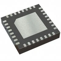
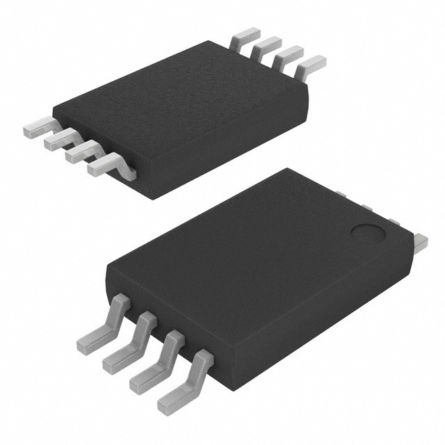
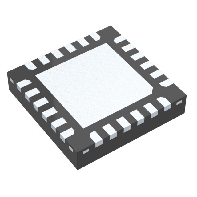
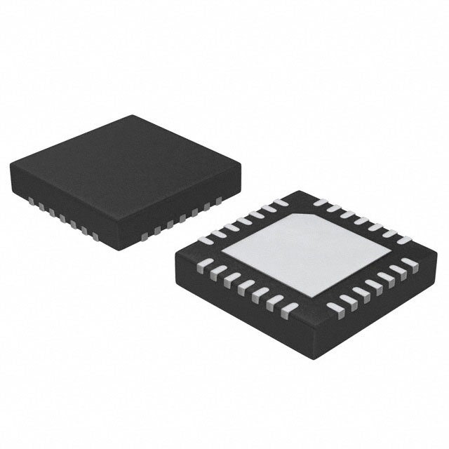
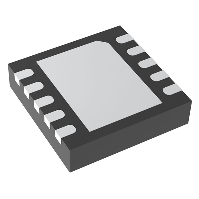
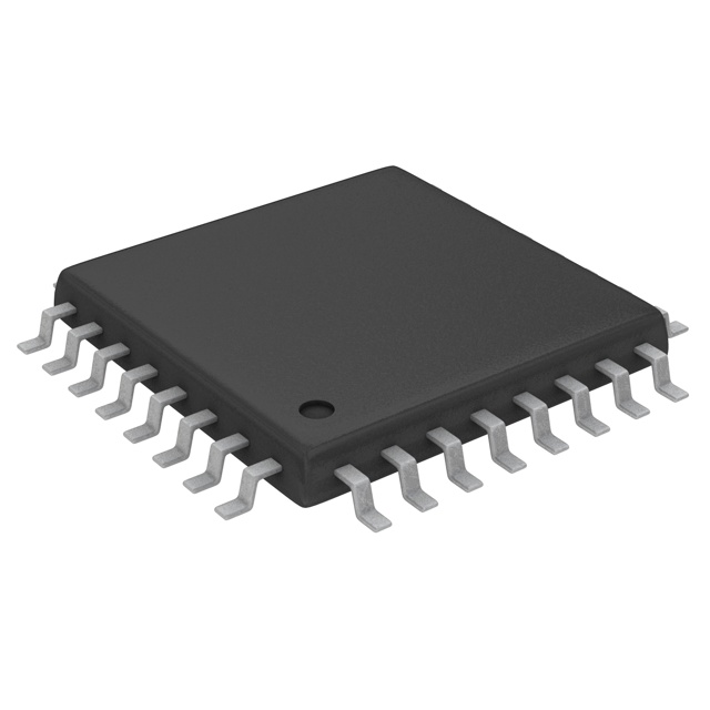
RF IC Fractional, Integer-N Synthesizer/VCO General Purpose 23.5 MHz ~ 6 GHz 32-TQFN (5x5)
- In stock 0

MAX2871ETJ+T – Complete Datasheet Summary
1. Basic Device Information
- Part Number: MAX2871ETJ+T
- Manufacturer: Maxim Integrated (Analog Devices)
- Device Type: Ultra-Wideband Fractional/Integer-N PLL Synthesizer with Integrated VCO
- Frequency Range: 23.5 MHz to 6000 MHz
- Core: Multi-band integrated VCO (3–6 GHz) + 1–128 dividers
- Package: 32-pin TQFN-EP (5 mm × 5 mm), TJ package
- Packing: Tape-and-reel (T suffix)
- RoHS/Lead-free: Compliant (+ suffix)
- Temperature Grade: Extended industrial −40°C to +85°C
- Logic Compatibility: 1.8V digital I/O
- Pin/Software Compatible: MAX2870
- Document: Rev 4, June 2020
2. Key Features
- Frequency coverage: 23.5 MHz–6 GHz using internal VCO and dividers
- Fractional-N & Integer-N operation
- Low normalized in-band phase noise: −230 dBc/Hz
- Dual differential programmable RF outputs
- Output power: −1 dBm to +8 dBm differential (per channel)
- Independent output mute & power control
- Fast lock + cycle-slip reduction
- Auto or manual VCO selection
- Phase adjustment / multi‑chip phase synchronization
- On-chip 7-bit temperature sensor + ADC
- On-chip 7-bit tune voltage ADC
- 4-wire SPI interface (3-wire write, 4-wire read)
- Low-phase-noise PFD up to 140 MHz
- Reference input up to 210 MHz
- Internal compensation; minimal external components
- Overtemperature & overvoltage protection
3. Electrical Specifications
Supply
| Parameter | Min | Typ | Max | Unit |
|---|---|---|---|---|
| Supply Voltage (VCC) | 3.0 | 3.3 | 3.6 | V |
| Total Supply Current (max power) | — | 165 | 200 | mA |
| Sleep Mode Current | — | — | 1 | mA |
Reference Input
| Parameter | Min | Typ | Max | Unit |
|---|---|---|---|---|
| REF_IN Frequency | 10 | — | 210 | MHz |
| Input Sensitivity | 0.7 | — | VCC | VPP |
| Input Capacitance | — | 2 | — | pF |
Phase Detector (PFD)
| Mode | Max Freq | Unit |
|---|---|---|
| Integer-N | 140 | MHz |
| Fractional-N | 125 | MHz |
RF Output
| Parameter | Value | Unit | |
|---|---|---|---|
| Fundamental VCO | 3000–6000 | MHz | |
| Divided Range | 23.4375–6000 | MHz | |
| Output Power (diff) | −1 to +8 | dBm | |
| Output Power (single-ended) | −4 to +5 | dBm | |
| Muted Isolation | — | −40 | dBc |
| Output Impedance | 50 | Ω |
Phase Noise (Typical)
表格
| VCO Frequency | 10 kHz | 100 kHz | 1 MHz | 5 MHz | Unit |
|---|---|---|---|---|---|
| 3 GHz | −83 | −111 | −136 | −149 | dBc/Hz |
| 4.5 GHz | −77 | −106 | −132 | −147 | dBc/Hz |
| 6 GHz | −71 | −101 | −128 | −144 | dBc/Hz |
Charge Pump
| Parameter | Min | Typ | Max | Unit |
|---|---|---|---|---|
| Sink/Source Current | 0.32 | — | 5.12 | mA |
| RSET Range | 2.7 | — | 10 | kΩ |
Digital I/O
| Parameter | Min | Max | Unit |
|---|---|---|---|
| VIL | — | 0.4 | V |
| VIH | 1.5 | — | V |
4. Absolute Maximum Ratings
- VCC to GND: −0.3 V to +3.9 V
- All other pins: −0.3 V to VCC + 0.3 V
- Continuous power dissipation: 2759 mW (TA ≤ 70°C)
- Junction temperature: +150°C
- Storage temperature: −65°C to +150°C
- Reflow temperature: +260°C
- ESD HBM: Class 1A
5. Thermal Data (32-pin TQFN-EP)
- θJA (junction-to-ambient): 29°C/W
- θJC (junction-to-case): 1.7°C/W
- Exposed pad must be soldered to PCB ground
6. Pin Configuration (32-Pin TQFN‑EP, Top View)
| Pin | Name | Function |
|---|---|---|
| 1 | CLK | SPI Clock |
| 2 | DATA | SPI Data In |
| 3 | LE | Load Enable |
| 4 | CE | Chip Enable |
| 5 | SW | Fast‑Lock Switch |
| 6 | VCC_CP | Charge Pump Supply |
| 7 | CP_OUT | Charge Pump Output |
| 8 | GND_CP | Charge Pump Ground |
| 9 | GND_PLL | PLL Ground |
| 10 | VCC_PLL | PLL Supply |
| 11 | GND_RF | RF Ground |
| 12 | RFOUTA_P | RF Out A+ |
| 13 | RFOUTA_N | RF Out A− |
| 14 | RFOUTB_P | RF Out B+ |
| 15 | RFOUTB_N | RF Out B− |
| 16 | VCC_RF | RF Supply |
| 17 | VCC_VCO | VCO Supply |
| 18 | GND_VCO | VCO Ground |
| 19 | NOISE_FILT | VCO Noise Filter |
| 20 | TUNE | VCO Tune Input |
| 21 | GND_TUNE | Tune Ground |
| 22 | RSET | CP Current Set Resistor |
| 23 | BIAS_FILT | Bias Filter |
| 24 | REG | Reference Regulator |
| 25 | LD | Lock Detect |
| 26 | RFOUT_EN | RF Output Enable |
| 27 | GND_DIG | Digital Ground |
| 28 | VCC_DIG | Digital Supply |
| 29 | REF_IN | Reference Input |
| 30 | MUX | Multiplexed I/O |
| 31 | GND_SD | Sigma‑Delta Ground |
| 32 | VCC_SD | Sigma‑Delta Supply |
| EP | Exposed Pad | Ground |
7. Functional Description
- Architecture: Integer‑N / Fractional‑N PLL with integrated wideband VCO
- VCO: 4 core VCOs covering 3–6 GHz, 16 sub‑bands each
- Output Dividers: 1, 2, 4, 8, 16, 32, 64, 128
- Dual Differential Outputs: Independent enable, power, mute
- Control: SPI (6 write registers, 1 read register)
- Lock Detect: Digital or analog; configurable precision
- Fast‑Lock: External pin (SW) enables fast‑lock filter topology
- Cycle‑Slip Reduction: Improves lock time
- Phase Sync: Supports multi‑chip phase synchronization
- Auto VCO Select (VAS): Automatically selects optimal VCO band
- Mute‑until‑Lock: Disables outputs until locked
8. Modes of Operation
- Integer‑N: INT = 1; low spurious
- Fractional‑N: INT = 0; fine frequency resolution
- Auto Integer: F01 = 1; auto‑switches to Integer when FRAC = 0
- Fast‑Lock: CDM = 01; reduces lock time
- Cycle‑Slip Reduction: CSM = 1; improves lock speed
- Phase Adjustment: CDM = 10; adjusts output phase
- Low‑Spur Mode: SDN = 10/11; reduces fractional spurs
- Low‑Noise Mode: SDN = 00; best phase noise
9. Application Circuit Requirements
- Loop filter between CP_OUT and TUNE
- RSET resistor (2.7–10 kΩ) from pin 22 to GND
- Decoupling caps on all VCC pins (≥0.1 µF ceramic)
- 1 µF caps on NOISE_FILT, BIAS_FILT, REG
- RF outputs: 50 Ω match; external choke or resistor to VCC_RF
- REF_IN: AC‑coupled
- MUX: Used for phase sync, monitor, or SPI readback
10. Typical Applications
- Wireless infrastructure
- Microwave radios
- Test & measurement
- Clock generator
- LoRa/Wi-Fi/Bluetooth systems
- Radar and sensor systems
- Point-to-point microwave
11. Ordering & Marking
- MAX2871ETJ+T: −40°C to +85°C, 32-pin TQFN-EP, tape-and-reel
- Package code: T3255+5
- Land pattern: 90-0013
- RoHS compliant, lead-free
Purchase
No need to register to order from JMChip Electronics, but signing in lets you track your order like a pro. Give it a try for a smoother shopping ride.
Means
Easy peasy! Pay your way with PayPal, Credit Card, or wire transfer in USD. We've got you covered.
RFQ(Request for Quotations)
Get the freshest prices and stock updates by asking for a quote! Our sales team will shoot you an email within a day. It's that simple.
IMPORTANT NOTICE
1. Look out for your order details in your inbox! (If it's missing, check the spam folder just in case.)
2. Our sales manager will double-check the order and keep you posted on any price or stock changes. No worries, we've got you covered.

Shipping Rate
We ship orders once a day around 5 p.m., except Sunday. Once shipped, the estimated delivery time depends on the courier company you choose, usually 5-7 working days.

Shipping Methods
We provide DHL, FedEx, UPS, EMS, SF Express, and Registered Air Mail international shipping.


Payment
You can pay the orders on the website directly or pay by wire transfer offline. We support: Paypal、VISA、Credit Card.


Analog Devices Inc./Maxim Integrated
Analog Devices Inc./Maxim Integrated
Analog Devices Inc./Maxim Integrated

Analog Devices Inc./Maxim Integrated
Analog Devices Inc./Maxim Integrated
Analog Devices Inc./Maxim Integrated
Analog Devices Inc./Maxim Integrated
Analog Devices Inc./Maxim Integrated
Analog Devices Inc./Maxim Integrated
Analog Devices Inc./Maxim Integrated
Analog Devices Inc./Maxim Integrated
Analog Devices Inc./Maxim Integrated