Sanyo NB3N111KMNG-SY


- Part Number:
NB3N111KMNG-SY
- Manufacturer:
- Category:
- RoHs:
 RoHS Compliant
 - Datasheet:
- Description:
3.3V DIFFERENTIAL 1:10 FANOUT CL
- In stock 148

NB3N111KMNG-SY Product Information Summary
Product Overview
- Manufacturer: ON Semiconductor
- Model: NB3N111KMNG-SY
- Description: 3.3V Differential 1:10 Fanout Clock Driver with HCSL Outputs
Features
- Typical Input Clock Frequency: 100, 133, 166, or 400 MHz
- Rise and Fall Times: 220 ps typical
- Propagation Delay: 800 ps typical
- Maximum Propagation Delay Variation per Differential Pair: 100 ps
- RMS Additive Phase Jitter: 0.1 ps typical
- LVDS Output Levels: Optional with interface termination
- Operating Range: VCC = 3.0 V to 3.6 V with GND = 0 V
- HCSL Output Levels: 700 mV peak-to-peak typical
- LVDS Output Levels: With interface termination
- Pb-Free Device
Applications
- Clock Distribution
- PCIe I, II, III
- Networking
- High End Computing
- Routers
- Servers
- FBDIMM Memory Card
Ordering Information
- Part Number: NB3N111KMNG-SY
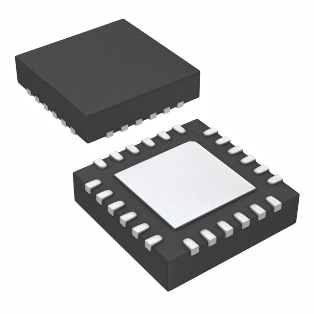
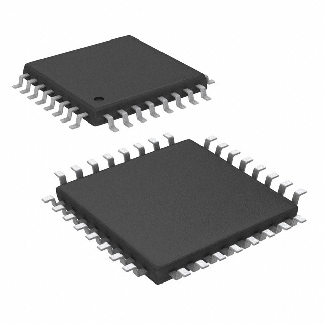
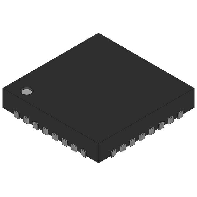
- Package: QFN32 (Pb-Free)
- Shipping: 74 Units / Rail
Pin Configuration
- IREF: Used to set the output drive. Connect a 475 Ω resistor from IREF to GND to produce 2.6 mA of IREF current.
- VTCLK, VTCLK-: Internal 50 Ω termination resistor connection pins.
- CLK: LVPECL, HCSL, LVDS Input (TRUE)
- CLK-: LVPECL, HCSL, LVDS Input (INVERT)
- Q[9-0]: HCSL or LVDS Output (TRUE and INVERT)
- GND: Supply Ground
- VCC: Positive Voltage Supply
- Exposed Pad (EP): GND Exposed Pad. Must be attached to a sufficient heat-sinking conduit and electrically connected to the circuit board ground (GND).
Electrical Characteristics
- ESD Protection:Human Body Model: >2 kVMachine Model: 200 V
- Moisture Sensitivity: QFN32 Level 1
- Flammability Rating: UL 94 V-0 @ 0.125 in
- Transistor Count: 286
- Meets or Exceeds JEDEC Spec EIA/JESD78 IC Latchup Test
Maximum Ratings
- VCC Positive Power Supply: 4.6 V (GND = 0 V)
- VI Positive Input: GND - 0.3 V to VCC (GND = 0 V)
- VINPP Differential Input Voltage: VCC
- IOUT Output Current: Continuous 50 mA, Surge 100 mA
- Operating Temperature Range: -40°C to +85°C
- Storage Temperature Range: -65°C to +150°C
- Thermal Resistance (Junction-to-Ambient): 31°C/W (0 lfpm), 27°C/W (500 lfpm)
- Thermal Resistance (Junction-to-Case): 12°C/W
DC Characteristics
- IGND GND Supply Current (All Outputs Loaded): 60 mA to 90 mA
- ICC Power Supply Current (All Outputs Loaded): 210 mA to 260 mA
- IIH Input HIGH Current: 2.0 µA to 150 µA
- IIL Input LOW Current: -150 µA to -2.0 µA
- RTIN Internal Input Termination Resistor: 45 Ω to 55 Ω
- Vth Input Threshold Reference Voltage Range: 350 mV to VCC - 1000 mV
- VIH Single-Ended Input HIGH Voltage: Vth + 150 mV to VCC
- VIL Single-Ended Input LOW Voltage: GND to Vth - 150 mV
- VIHD Differential Input HIGH Voltage: 425 mV to VCC - 850 mV
- VILD Differential Input LOW Voltage: GND to VCC - 1000 mV
- VID Differential Input Voltage: 150 mV to VCC - 850 mV
- VCMR Input Common Mode Range: 350 mV to VCC - 1000 mV
- VOH Output HIGH Voltage (HCSL): 600 mV to 900 mV
- VOL Output LOW Voltage (HCSL): -150 mV to 150 mV
AC Characteristics
- VOUTPP Output Voltage Amplitude (@ VINPPmin): 725 mV to 1000 mV (fin ≤ 400 MHz)
- Propagation Delay (tPLH, tPHL): 550 ps to 1100 ps
- Propagation Delay Variation (ΔtPLH, ΔtPHL): 100 ps
- Duty Cycle Skew (tSKEW): 20 ps to 150 ps
- Additive Integrated Phase Jitter (tJIT): 0.1 ps at Fc = 100 MHz
- Input Voltage Swing/Sensitivity (Differential Configuration): 0.150 V to VCC - 0.85 V
- Absolute Crossing Magnitude Voltage (VCROSS): 250 mV to 550 mV
- Variation in Magnitude of VCROSS (ΔVCROSS): 150 mV
- Output Risetime and Falltime (tr, tf): 150 ps to 400 ps
- Variation in Magnitude of Risetime and Falltime (Δtr, Δtf): 125 ps
Package Dimensions
- QFN32 5x5x1.0 mm: See detailed dimensions in the datasheet.
Purchase
No need to register to order from JMChip Electronics, but signing in lets you track your order like a pro. Give it a try for a smoother shopping ride.
Means
Easy peasy! Pay your way with PayPal, Credit Card, or wire transfer in USD. We've got you covered.
RFQ(Request for Quotations)
Get the freshest prices and stock updates by asking for a quote! Our sales team will shoot you an email within a day. It's that simple.
IMPORTANT NOTICE
1. Look out for your order details in your inbox! (If it's missing, check the spam folder just in case.)
2. Our sales manager will double-check the order and keep you posted on any price or stock changes. No worries, we've got you covered.

Shipping Rate
We ship orders once a day around 5 p.m., except Sunday. Once shipped, the estimated delivery time depends on the courier company you choose, usually 5-7 working days.

Shipping Methods
We provide DHL, FedEx, UPS, EMS, SF Express, and Registered Air Mail international shipping.


Payment
You can pay the orders on the website directly or pay by wire transfer offline. We support: Paypal、VISA、Credit Card.