
onsemi NCV20082DMR2G


- Part Number:
NCV20082DMR2G
- Manufacturer:
- Category:
- RoHs:
 RoHS Compliant
 - Datasheet:
 NCV20082DMR2G_Datesheet
 - Description:
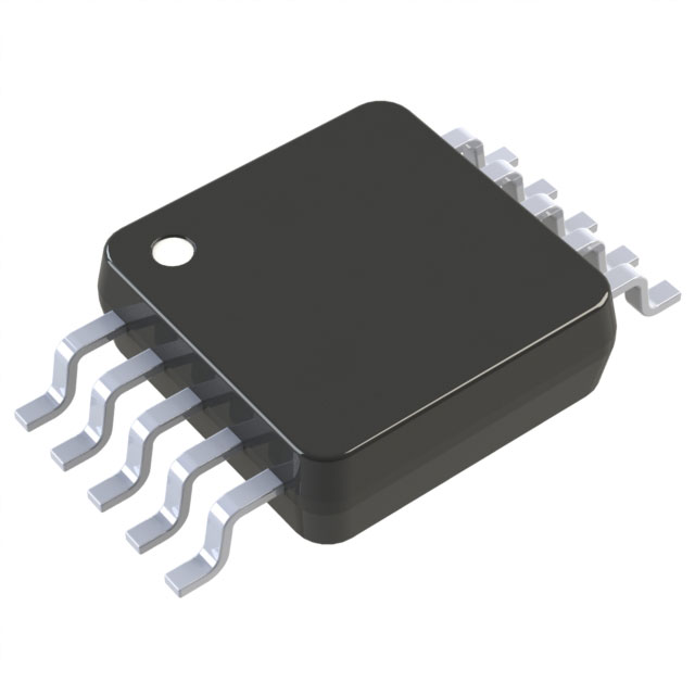
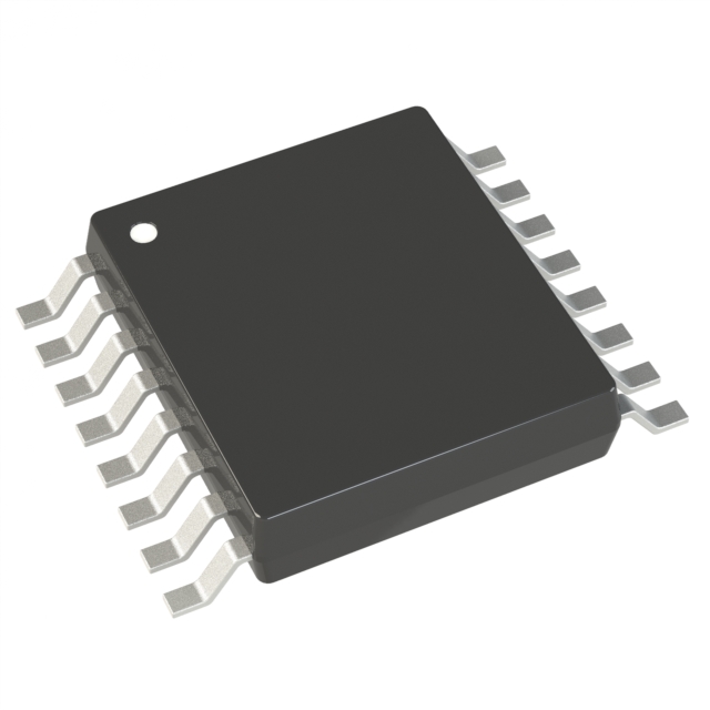
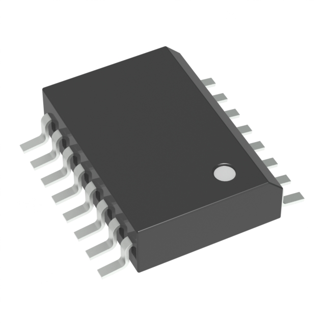
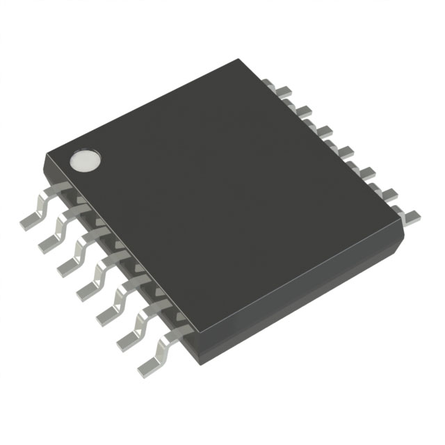
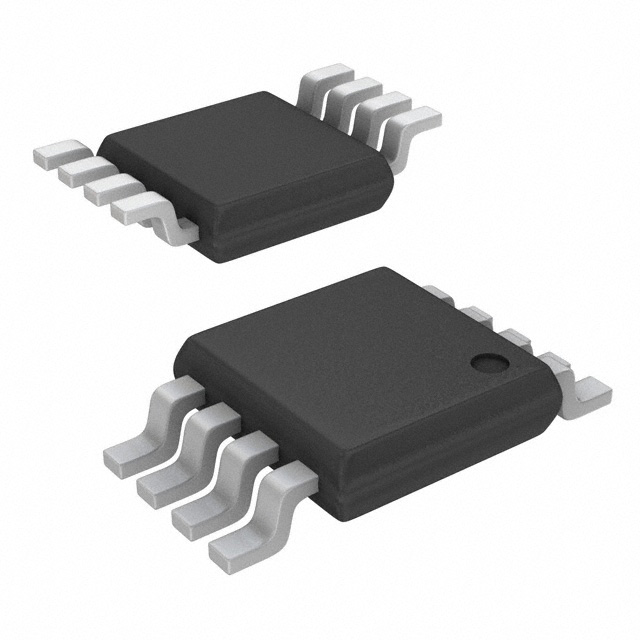
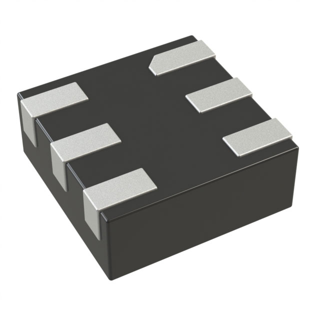
IC OPAMP GP 2 CIRCUIT 8MSOP
- In stock 7,700

Overview
The NCV20082DMR2G is a part of the NCS20081/2/4 family, a series of single, dual, and quad Operational Amplifiers (Op Amps) designed for low power consumption and high performance. This specific model is a dual channel configuration, featuring a 1.2 MHz Gain-Bandwidth Product (GBWP) while consuming only 42 µA of Quiescent current per opamp.
Key Features
- Wide Bandwidth: 1.2 MHz
- Low Supply Current: 42 µA typical per channel (VS = 1.8 V)
- Low Input Offset Voltage: 4 mV maximum
- Wide Supply Range: 1.8 V to 5.5 V
- Wide Temperature Range: −40°C to +125°C
- Rail-to-Rail Input and Output
- Unity Gain Stable
- AEC-Q100 Qualified: Denoted by the NCV prefix
- Pb-Free, Halogen Free/BFR Free, and RoHS Compliant
Applications
- Automotive
- Battery Powered/Portable
- Sensor Signal Conditioning
- Low Voltage Current Sensing
- Filter Circuits
- Unity Gain Buffer
Electrical Characteristics
- Input Offset Voltage: 0.5 to 3.5 mV
- Offset Voltage Drift: 1 µV/°C
- Input Bias Current: 1 pA to 1500 pA
- Input Offset Current: 1 pA to 1100 pA
- Common Mode Rejection Ratio (CMRR): 45 to 73 dB
- Open Loop Voltage Gain: 86 to 120 dB
- Short Circuit Current: 15 mA (sinking), 11 mA (sourcing)
- Output Voltage High (VOH): 3 to 24 mV
- Output Voltage Low (VOL): 3 to 24 mV
- Unity Gain Bandwidth: 1.2 MHz
- Slew Rate at Unity Gain: 0.4 V/µs
- Power Supply Quiescent Current (IDD): 42 µA per channel
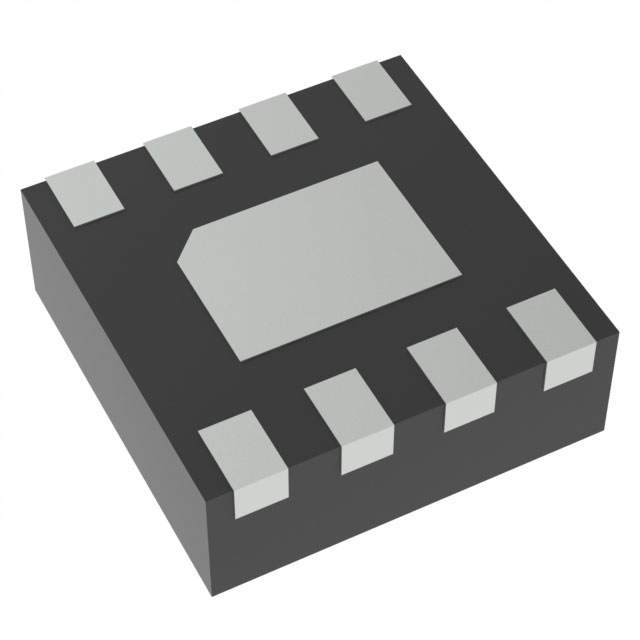
Mechanical Data
- Case: Micro8/MSOP8
- Marking: 2K82
Absolute Maximum Ratings
- Supply Voltage (VDD – VSS): 6 V
- Input Voltage (VI): VSS − 0.5 to VDD + 0.5 V
- Differential Input Voltage (VID): ±Vs
- Maximum Input Current (I): ±10 mA
- Maximum Output Current (IO): ±100 mA
- Continuous Total Power Dissipation (PD): 200 mW
- Maximum Junction Temperature (TJ): 150 °C
- Storage Temperature Range (TSTG): −65 to 150 °C
- Mounting Temperature (Tmount): 260 °C
Thermal Information
- Junction to Ambient Thermal Resistance (°C/W): 236 for Single Layer Board, 167 for Multi-Layer Board
Operating Ranges
- Operating Supply Voltage (VS): 1.8 to 5.5 V
- Differential Input Voltage (VID): VS V
- Input Common Mode Range (VICM): VSS – 0.2 VDD + 0.2 V
- Ambient Temperature (TA): −40 to 125 °C
Purchase
No need to register to order from JMChip Electronics, but signing in lets you track your order like a pro. Give it a try for a smoother shopping ride.
Means
Easy peasy! Pay your way with PayPal, Credit Card, or wire transfer in USD. We've got you covered.
RFQ(Request for Quotations)
Get the freshest prices and stock updates by asking for a quote! Our sales team will shoot you an email within a day. It's that simple.
IMPORTANT NOTICE
1. Look out for your order details in your inbox! (If it's missing, check the spam folder just in case.)
2. Our sales manager will double-check the order and keep you posted on any price or stock changes. No worries, we've got you covered.

Shipping Rate
We ship orders once a day around 5 p.m., except Sunday. Once shipped, the estimated delivery time depends on the courier company you choose, usually 5-7 working days.

Shipping Methods
We provide DHL, FedEx, UPS, EMS, SF Express, and Registered Air Mail international shipping.


Payment
You can pay the orders on the website directly or pay by wire transfer offline. We support: Paypal、VISA、Credit Card.


onsemi
onsemi
onsemi
onsemi
onsemi
onsemi
onsemi
onsemi
onsemi
onsemi
onsemi

onsemi