NXP PMDXB1200UPEZ


- Part Number:
PMDXB1200UPEZ
- Manufacturer:
- Category:
- RoHs:
 Non-RoHS Compliant
 - Datasheet:
- Description:
MOSFET 30V
- In stock 1,798,650

PMDXB1200UPEZ Product Information Summary
1. General Description
The PMDXB1200UPEZ is a dual P-channel enhancement mode Field-Effect Transistor (FET) developed by Nexperia. It adopts Trench MOSFET technology and is housed in a leadless ultra-small DFN1010B-6 (SOT1216) surface-mounted device (SMD) plastic package. With a compact form factor and reliable performance, it is designed for low-voltage, medium-current switching applications, complying with relevant industry standards and specifications.
2. Core Features and Benefits
- Low Threshold Voltage: Enables efficient switching control with low drive voltage requirements.
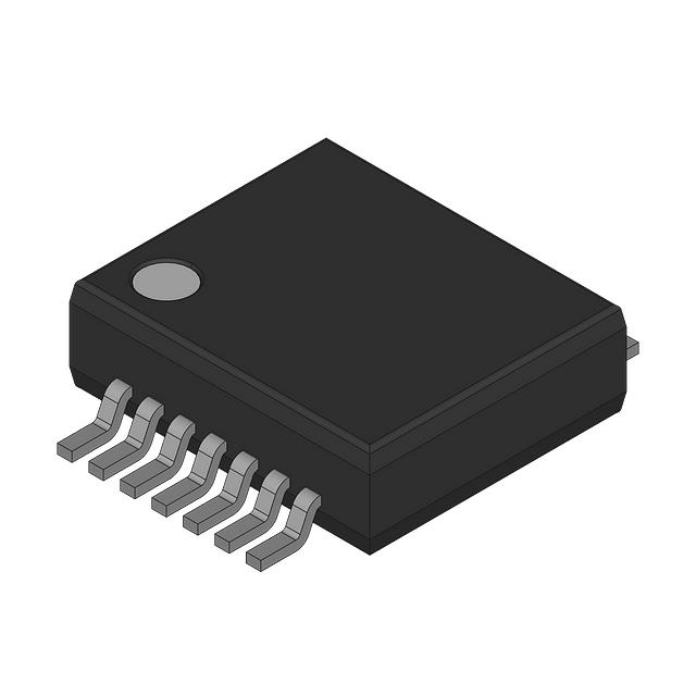
- Ultra-Compact Package: Measures 1.1 x 1.0 x 0.37 mm (DFN1010B-6/SOT1216), ideal for space-constrained designs.
- Trench MOSFET Technology: Delivers excellent electrical performance, including low on-state resistance and high switching speed.
- Robust ESD Protection: Withstands electrostatic discharge (ESD) greater than 2 kV (HBM), enhancing reliability in harsh environments.
- Dual Transistor Integration: Two independent P-channel MOSFETs in one package, reducing component count and PCB space.
3. Applications
- Relay driver circuits
- High-speed line driver applications
- High-side loadswitch implementations
- General-purpose switching circuits
4. Quick Reference Data (Per Transistor)
| Symbol | Parameter | Conditions | Min | Typ | Max | Unit |
|---|---|---|---|---|---|---|
| VDS | Drain-source voltage | Tj = 25 °C | - | - | -30 | V |
| VGS | Gate-source voltage | - | -8 | - | 8 | V |
| ID | Drain current | VGS = -4.5 V; Tamb = 25 °C [1] | - | - | -410 | mA |
| RDSon | Drain-source on-state resistance | VGS = -4.5 V; ID = -410 mA; Tj = 25 °C | - | 1.2 | 1.4 | Ω [1] Device mounted on an FR4 PCB (single-sided copper, tin-plated) with a 1 cm² drain mounting pad. |
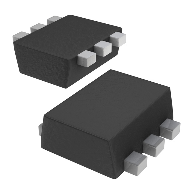
5. Pinning Information
5.1 Pin Configuration (DFN1010B-6/SOT1216 Package)
| Pin Number | Symbol | Description |
|---|---|---|
| 1 | S1 | Source of Transistor 1 (TR1) |
| 2 | G1 | Gate of Transistor 1 (TR1) |
| 3 | D2 | Drain of Transistor 2 (TR2) |
| 4 | S2 | Source of Transistor 2 (TR2) |
| 5 | G2 | Gate of Transistor 2 (TR2) |
| 6 | D1 | Drain of Transistor 1 (TR1) |
| 7 | D1 | Drain of Transistor 1 (TR1) [Duplicate pin] |
| 8 | D2 | Drain of Transistor 2 (TR2) [Duplicate pin] |
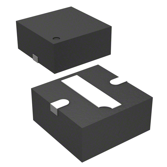
5.2 Package Outline
- Type: DFN1010B-6 (SOT1216)
- Leadless plastic thermal enhanced ultra-thin small outline package
- Dimensions (mm, nominal): 1.1 (length) x 1.0 (width) x 0.37 (height)
- Pin 1 index area for easy orientation during assembly
6. Ordering Information
| Type Number | Package | Package Description | Version |
|---|---|---|---|
| PMDXB1200UPEZ | DFN1010B-6 | Plastic thermal enhanced ultra-thin small outline package; no leads; 6 terminals | SOT1216 |
7. Marking Information
- Marking Code: 11 10 00 (binary marking code)
- Reading Direction: Refer to the pin 1 indication mark on the package
- Mark-free area is provided for assembly and inspection
8. Limiting Values (Per Transistor, IEC 60134 Absolute Maximum Rating System)
| Symbol | Parameter | Conditions | Min | Max | Unit |
|---|---|---|---|---|---|
| VDS | Drain-source voltage | Tj = 25 °C | - | -30 | V |
| VGS | Gate-source voltage | - | -8 | 8 | V |
| ID | Continuous drain current | VGS = -4.5 V; Tamb = 25 °C [1] | - | -410 | mA |
| ID | Continuous drain current | VGS = -4.5 V; Tamb = 100 °C [1] | - | -260 | mA |
| IDM | Peak drain current | Tamb = 25 °C; single pulse; tp ≤ 10 µs | - | -1.7 | A |
| Ptot | Total power dissipation | Tamb = 25 °C [2] | - | 285 | mW |
| Ptot | Total power dissipation | Tsp = 25 °C [1] | - | 410 | mW |
| Ptot | Total power dissipation | - [Special condition] | - | 4030 | mW |
| IS | Source current (source-drain diode) | Tamb = 25 °C [1] | - | -410 | mA |
| Tj | Junction temperature | - | -55 | 150 | °C |
| Tamb | Ambient temperature | - | -55 | 150 | °C |
| Tstg | Storage temperature | - | -65 | 150 | °C [1] Device mounted on an FR4 PCB (single-sided copper, tin-plated) with a 1 cm² drain mounting pad.[2] Device mounted on an FR4 PCB (single-sided copper, tin-plated) with standard footprint. |
9. Thermal Characteristics
| Symbol | Parameter | Conditions | Min | Typ | Max | Unit |
|---|---|---|---|---|---|---|
| Rth(j-a) | Thermal resistance (junction to ambient) | Free air [2] | - | 380 | 440 | K/W |
| Rth(j-a) | Thermal resistance (junction to ambient) | Free air [1] | - | 275 | 305 | K/W |
| Rth(j-sp) | Thermal resistance (junction to solder point) | - | - | 27 | 31 | K/W [1] Device mounted on an FR4 PCB (single-sided copper, tin-plated) with a 1 cm² drain mounting pad.[2] Device mounted on an FR4 PCB (single-sided copper, tin-plated) with standard footprint. |
10. Electrical Characteristics (Per Transistor, Tj = 25 °C Unless Stated Otherwise)
10.1 Static Characteristics
| Parameter | Conditions | Min | Typ | Max | Unit |
|---|---|---|---|---|---|
| Drain leakage current (IDSS) | VDS = -30 V; VGS = 0 V | - | - | -1 | µA |
| Gate leakage current (IGSS) | VGS = 8 V; VDS = 0 V | - | - | 5 | µA |
| Gate leakage current (IGSS) | VGS = -8 V; VDS = 0 V | - | - | -5 | µA |
| Gate leakage current (IGSS) | VGS = 4.5 V; VDS = 0 V | - | - | 1 | µA |
| Gate leakage current (IGSS) | VGS = -4.5 V; VDS = 0 V | - | - | -1 | µA |
| Gate leakage current (IGSS) | VGS = 2.5 V; VDS = 0 V | - | - | 100 | nA |
| Gate leakage current (IGSS) | VGS = -2.5 V; VDS = 0 V | - | - | -100 | nA |
| Drain-source on-state resistance (RDSon) | VGS = -4.5 V; ID = -410 mA | - | 1.2 | 1.4 | Ω |
| Drain-source on-state resistance (RDSon) | VGS = -4.5 V; ID = -410 mA; Tj = 150 °C | - | 2 | 2.4 | Ω |
| Drain-source on-state resistance (RDSon) | VGS = -2.5 V; ID = -320 mA | - | 1.7 | 2.3 | Ω |
| Drain-source on-state resistance (RDSon) | VGS = -1.8 V; ID = -80 mA | - | 2.1 | 3.1 | Ω |
| Drain-source on-state resistance (RDSon) | VGS = -1.5 V; ID = -10 mA | - | 3 | 5.1 | Ω |
| Forward transconductance (gfs) | VDS = -10 V; ID = -410 mA | - | 820 | - | mS |
| Gate-source threshold voltage (VGS(th)) | ID = -250 μA; VDS = VGS | - | - | - | V |
10.2 Dynamic Characteristics
| Parameter | Conditions | Min | Typ | Max | Unit |
|---|---|---|---|---|---|
| Total gate charge (QG) | VDS = -15 V; ID = -410 mA; VGS = -4.5 V | - | 0.7 | 1.2 | nC |
| Gate-source charge (QGS) | VDS = -15 V; ID = -410 mA; VGS = -4.5 V | - | 0.17 | - | nC |
| Gate-drain charge (QGD) | VDS = -15 V; ID = -410 mA; VGS = -4.5 V | - | 0.16 | - | nC |
| Input capacitance (Ciss) | VDS = -15 V; f = 1 MHz; VGS = 0 V | - | 43.2 | - | pF |
| Output capacitance (Coss) | VDS = -15 V; f = 1 MHz; VGS = 0 V | - | 5.9 | - | pF |
| Reverse transfer capacitance (Crss) | VDS = -15 V; f = 1 MHz; VGS = 0 V | - | 4.2 | - | pF |
| Turn-on delay time (td(on)) | VDS = -15 V; ID = -410 mA; VGS = -4.5 V; RG(ext) = 6 Ω | - | 3 | - | ns |
| Rise time (tr) | VDS = -15 V; ID = -410 mA; VGS = -4.5 V; RG(ext) = 6 Ω | - | 4 | - | ns |
| Turn-off delay time (td(off)) | VDS = -15 V; ID = -410 mA; VGS = -4.5 V; RG(ext) = 6 Ω | - | 14 | - | ns |
| Fall time (tf) | VDS = -15 V; ID = -410 mA; VGS = -4.5 V; RG(ext) = 6 Ω | - | 5 | - | ns |
10.3 Source-Drain Diode Characteristics
| Parameter | Conditions | Min | Typ | Max | Unit |
|---|---|---|---|---|---|
| Source-drain voltage (VSD) | IS = -410 mA; VGS = 0 V | - | -0.95 | -1.2 | V |
11. Soldering and Footprint
- Package Footprint: Designed for reflow soldering; refer to the recommended solder land dimensions (1.1 x 1.0 mm base with specific pad layouts for terminals).
- Soldering Guidelines: Follow standard SMD reflow soldering processes, ensuring proper thermal profiling to avoid package damage.
- PCB Mounting: Use the specified FR4 PCB with single-sided copper and tin-plating for optimal thermal and electrical performance.
Purchase
No need to register to order from JMChip Electronics, but signing in lets you track your order like a pro. Give it a try for a smoother shopping ride.
Means
Easy peasy! Pay your way with PayPal, Credit Card, or wire transfer in USD. We've got you covered.
RFQ(Request for Quotations)
Get the freshest prices and stock updates by asking for a quote! Our sales team will shoot you an email within a day. It's that simple.
IMPORTANT NOTICE
1. Look out for your order details in your inbox! (If it's missing, check the spam folder just in case.)
2. Our sales manager will double-check the order and keep you posted on any price or stock changes. No worries, we've got you covered.

Shipping Rate
We ship orders once a day around 5 p.m., except Sunday. Once shipped, the estimated delivery time depends on the courier company you choose, usually 5-7 working days.

Shipping Methods
We provide DHL, FedEx, UPS, EMS, SF Express, and Registered Air Mail international shipping.


Payment
You can pay the orders on the website directly or pay by wire transfer offline. We support: Paypal、VISA、Credit Card.