onsemi BSS138


- Part Number:
BSS138
- Manufacturer:
- Category:
- RoHs:
 RoHS Compliant
 - Datasheet:
 BSS138_Datesheet
 - Description:
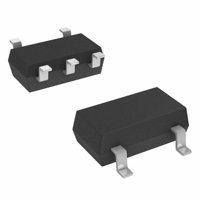
MOSFET N-CH 50V 220MA SOT23-3
- In stock 56,062

BSS138 Product Summary
Basic Information
- Part Number: BSS138
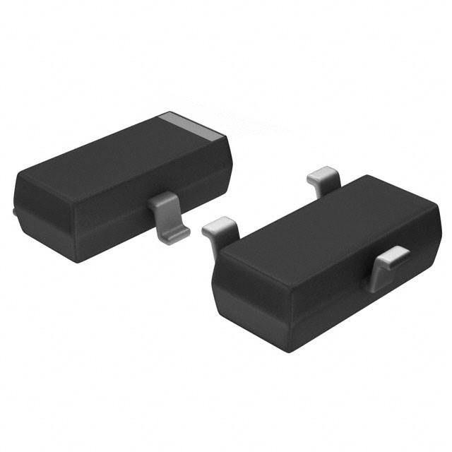
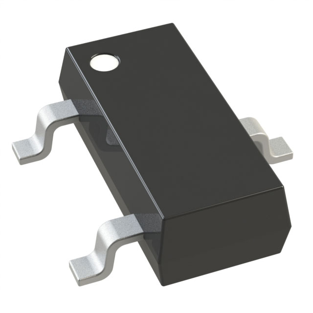
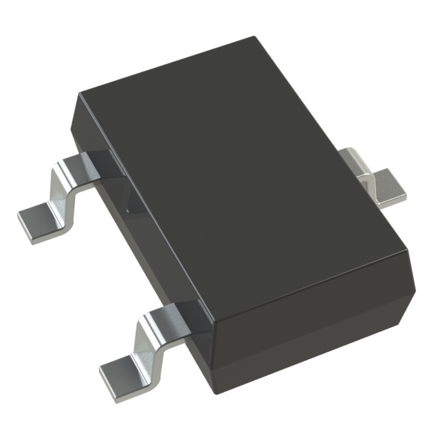
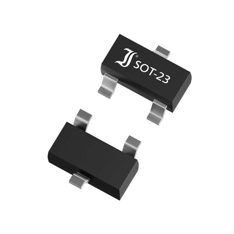
- Package Type: SOT-23-3 (Pb-Free)
- Shipping Quantity: 3000 per Tape & Reel
- Case Style: CASE 318-08
General Description
The BSS138 is an N-Channel enhancement mode field effect transistor produced using onsemi's proprietary, high cell density, DMOS technology. These transistors are designed to minimize on-state resistance while providing rugged, reliable, and fast switching performance. They are particularly suited for low voltage, low current applications such as small servo motor control, power MOSFET gate drivers, and other switching applications.
Features
- Drain-Source Voltage (VDS): 50 V
- Drain Current (ID):Continuous: 0.22 APulsed: 0.88 A
- On-State Resistance (RDS(on)):3.5 Ω @ VGS = 10 V6.0 Ω @ VGS = 4.5 V
- High Density Cell Design for Extremely Low RDS(on)
- Rugged and Reliable
- Compact Industry Standard SOT-23 Surface Mount Package
- ESD Protection: HBM Class 0A, MM Class M2
- Pb-Free and Halogen-Free
Marking Diagram & Pin Assignment
- Device Code: SS
- Date Code: M
- Pb-Free Package Indicator: �
- Pin Configuration:Pin 1: GatePin 2: SourcePin 3: Drain
Ordering Information
- BSS138: SOT-23-3 (Pb-Free) 3000 / Tape & Reel
- BSS138-G: SOT-23-3 (Pb-Free) 3000 / Tape & Reel
Absolute Maximum Ratings (@TA = 25°C, unless otherwise noted)
- Drain-Source Voltage (VDSS): 50 V
- Gate-Source Voltage (VGSS): ±20 V
- Drain Current (ID):Continuous: 0.22 APulsed: 0.88 A
- Maximum Power Dissipation (PD): 0.36 W
- Derate Above 25°C: 2.8 mW/°C
- Operating and Storage Junction Temperature Range (TJ, TSTG): -55 to +150 °C
- Maximum Lead Temperature for Soldering Purposes (TL): 300 °C
Thermal Characteristics (@TA = 25°C, unless otherwise noted)
- Thermal Resistance, Junction-to-Ambient (RθJA): 350 °C/W
Electrical Characteristics (@TA = 25°C, unless otherwise noted)
- OFF CHARACTERISTICS:Drain-Source Breakdown Voltage (V(BR)DSS): 50 V (VGS = 0 V, ID = 250 µA)Zero Gate Voltage Drain Current (IDSS):VDS = 50 V, VGS = 0 V: 0.5 µAVDS = 50 V, VGS = 0 V, TJ = 125°C: 5 µAVDS = 30 V, VGS = 0 V: 100 nAGate-Body Leakage Current (IGSS): ±100 nA (VGS = ±20 V, VDS = 0 V)
- ON CHARACTERISTICS:Gate Threshold Voltage (VGS(th)): 0.8 to 1.5 V (VDS = VGS, ID = 1 mA)Static Drain-Source On-Resistance (RDS(on)):VGS = 10 V, ID = 0.22 A: 0.7 to 3.5 ΩVGS = 4.5 V, ID = 0.22 A: 1.0 to 6.0 ΩVGS = 10 V, ID = 0.22 A, TJ = 125°C: 1.1 to 5.8 ΩOn-State Drain Current (ID(on)): 0.2 A (VGS = 10 V, VDS = 5 V)Forward Transconductance (gFS): 0.12 to 0.5 S (VDS = 10 V, ID = 0.22 A)
- DYNAMIC CHARACTERISTICS:Input Capacitance (Ciss): 27 pF (VDS = 25 V, VGS = 0 V, f = 1.0 MHz)Output Capacitance (Coss): 13 pFReverse Transfer Capacitance (Crss): 6 pFGate Resistance (RG): 9 Ω (VGS = 15 mV, f = 1.0 MHz)
- SWITCHING CHARACTERISTICS:Turn-On Delay Time (td(on)): 2.5 to 5 ns (VDD = 30 V, ID = 0.29 A, VGS = 10 V, RGEN = 6 Ω)Turn-On Rise Time (tr): 9 to 18 nsTurn-Off Delay Time (td(off)): 20 to 36 nsTurn-Off Fall Time (tf): 7 to 14 nsTotal Gate Charge (Qg): 1.7 to 2.4 nC (VDS = 25 V, ID = 0.22 A, VGS = 10 V)Gate-Source Charge (Qgs): 0.1 nCGate-Drain Charge (Qgd): 0.4 nC
- DRAIN-SOURCE DIODE CHARACTERISTICS AND MAXIMUM RATINGS:Maximum Continuous Drain-Source Diode Forward Current (IS): 0.22 ADrain-Source Diode Forward Voltage (VSD): 0.8 to 1.4 V (VGS = 0 V, IS = 0.44 A)
Typical Electrical Characteristics
- On-Region Characteristics: See Figure 1
- On-Resistance Variation with Drain Current and Gate Voltage: See Figure 2
- On-Resistance Variation with Temperature: See Figure 3
- On-Resistance Variation with Gate-to-Source Voltage: See Figure 4
- Transfer Characteristics: See Figure 5
- Body Diode Forward Voltage Variation with Source Current and Temperature: See Figure 6
- Gate Charge Characteristics: See Figure 7
- Capacitance Characteristics: See Figure 8
- Maximum Safe Operating Area: See Figure 9
- Single Pulse Maximum Power Dissipation: See Figure 10
- Transient Thermal Response Curve: See Figure 11
Mechanical Case Outline Package Dimensions
- SOT-23 (TO-236): 2.90x1.30x1.00 mm
- Pin Configuration:Pin 1: GatePin 2: SourcePin 3: Drain
Purchase
No need to register to order from JMChip Electronics, but signing in lets you track your order like a pro. Give it a try for a smoother shopping ride.
Means
Easy peasy! Pay your way with PayPal, Credit Card, or wire transfer in USD. We've got you covered.
RFQ(Request for Quotations)
Get the freshest prices and stock updates by asking for a quote! Our sales team will shoot you an email within a day. It's that simple.
IMPORTANT NOTICE
1. Look out for your order details in your inbox! (If it's missing, check the spam folder just in case.)
2. Our sales manager will double-check the order and keep you posted on any price or stock changes. No worries, we've got you covered.

Shipping Rate
We ship orders once a day around 5 p.m., except Sunday. Once shipped, the estimated delivery time depends on the courier company you choose, usually 5-7 working days.

Shipping Methods
We provide DHL, FedEx, UPS, EMS, SF Express, and Registered Air Mail international shipping.


Payment
You can pay the orders on the website directly or pay by wire transfer offline. We support: Paypal、VISA、Credit Card.


onsemi
onsemi
onsemi
onsemi
onsemi
onsemi

onsemi
onsemi
onsemi
onsemi
onsemi

onsemi